1. Introduction
Transparent conductive oxides (TCOs) are a family of functional materials that have received considerable attention in the last few years due to their potential optoelectronic applications. Among their main advantages, TCOs have awakened attention because these semiconductor oxides have an energy band gap between 3 and 5 eV combined with a relatively high electrical conduction, due to the presence of point defects [
1]. These qualities make TCOs both, conductors and transparent to visible light. Some of the most studied oxides in this family of materials are In
2O
3, SnO
2, Ga
2O
3, ZnO, among others. However, recent studies warn about the use of critical elements like In, Ga, Ge, etc., in TCOs attending to economic reasons and supply risk in optoelectronic devices [
2]. Therefore, in order to reduce the amount of the crucial elements while maintaining their functionality, the search for novel materials goes through the synthesis of superstructures resulting from the intergrowth of two structural types. In this sense, the homologous series of indium zinc oxides (IZO), with chemical formula Zn
kIn
2O
k+3, keeps its conductivity values and high transmittance in the visible region [
3] while satisfying the requirements for decreasing indium content with respect to the binary oxides and also others ternary oxides, like the well-known In-Sn-O (ITO). Additionally, the tunable electrical, photocatalytic, thermoelectric and luminescent properties as a function of the ZnO content (
k value) widen the potential applications of the IZOs series as TCOs [
3,
4,
5,
6].
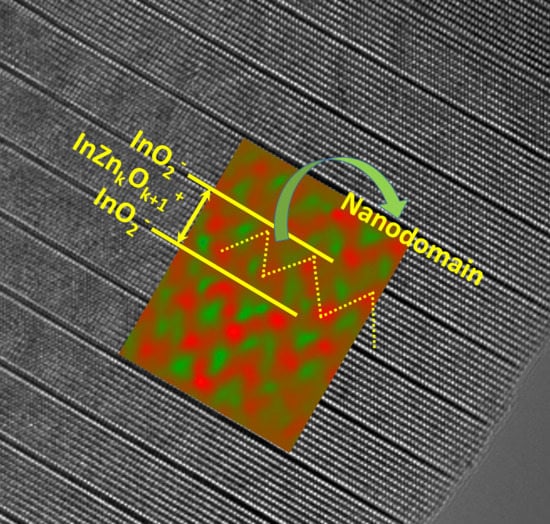
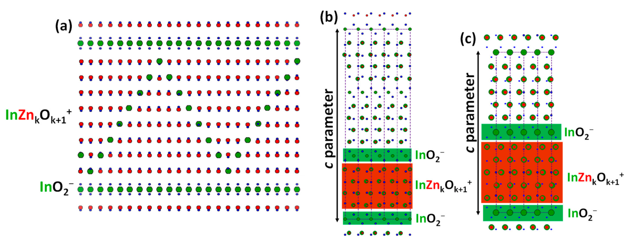
The structure of IZOs consists of an ordered intergrowth of InO
2- layers in octahedral coordination (hereinafter referred to as In–O layers) and wurtzite-like InZn
kO
k+1+ blocks, where indium and zinc occupy trigonal bipyramidal and tetrahedral sites, respectively, (for the sake of simplicity referred to as In/Zn–O blocks) stacked along the
c-axis (
Figure 1a). The symmetry of the homologous series Zn
kIn
2O
k+3 can be described according to the
R-3
m spatial group for
k odd values, while
k even terms can be characterized with the spatial group
P6
3/
mm [
7,
8]. This is because, in odd
k terms, the
c parameter comprises the distance between 3 consecutive In-O layers, whereas, in
k even members only, 2 consecutive In-O layers are included.
Figure 1b,c shows the schematic structural representation of
k = 3 and
k = 4 members along the [010] direction, where the
c parameter is indicated. For terms with
k ≥ 6 a modulation showing a zig-zag or a wave-like shape has been observed by transmission electron microscopy (TEM) [
9,
10,
11]. This modulation consists of an inhomogeneous distribution of the In
3+ nanoclusters inside the wurtzite blocks following a zig-zag pattern in order to minimize the internal deformation produced by the different ionic radii of In
3+ (0.80 Å) and Zn
2+ (0.60 Å) [
12]. The modulation for terms with
k < 6 has been more recently identified, although no systematic studied has been performed to date [
6]. In summary, IZOs are emerging as commercially viable transparent conducting oxides because of its excellent optical transmission, good electrical conductivity and high chemical and thermal stability, whose characteristic atomic distribution plays an important role in the electronic properties [
13,
14].
The origin of the zig-zag modulation on IZO nanowires was studied by Goldstein et al. [
15] using spherical aberration (Cs)-corrected microscopy by scanning TEM mode and density functional theory (DFT) calculations. These authors suggested that the zig-zag of In
3+ arises from an inversion of the metal and oxygen positions on both sides of the In
3+ trigonal bipyramidal positions within the wurtzite block. Their model reveals that this defect runs along the {1-21
l} planes of the wurtzite structure, being the most stable computed value
l = 3. According to their results, the calculated angle formed by the intersection of the zig-zag plane and the In-O layer is 46.8°. Nevertheless, the nature of this modulation has been the subject of intense debate during the last years [
15,
16,
17,
18]. Indeed, previous studies showed a clear influence of the nature of M
3+ on the modulation. Actually, when In
3+ is replaced by Fe
3+ the angle and periodicity of the zig-zag is modified [
11,
15,
16,
17,
18], and when In
3+ is replaced by Ga
3+ or Al
3+, the zig-zag modulation disappears, placing both cations in the middle of the block [
19]. However, there are not details about the influence of the In
3+ distribution in the wurtzite-block as a function of the
k term and most notable is the lack of information on the lower members of this homologous series. In this work, we focus on the effect that the zig-zag distribution of In
3+ causes on the wurtzite-like InZn
kO
k+1+ blocks as a function of the
k term, with special attention to those terms with a low
k value. For this propose, we have carried out an exhaustive study of the In
3+ modulation in three different terms of the series (
k = 3, 7 and 11) and we have evaluated the lattice deformation caused by the In
3+ within the wurtzite-type block by exploiting the capabilities offered by aberration-corrected (S)TEM operating at low electron dose to prevent In
3+ from diffusing.
2. Materials and Methods
The three terms of the homologous series Zn
kIn
2O
k+3 (
k = 3, 7, and 11) were obtained by conventional solid state reactions. A mixture of appropriate amounts of the constituent oxides ZnO (Aldrich, St. Louis, Missouri, USA, 99.99%) and In
2O
3 (Aldrich, St. Louis, Missouri, USA, 99.99%) was treated under different thermal conditions depending on the
k value in order to avoid the formation of impurities and disordered intergrowths of different terms. In this regard, we prepared all samples at 1350 °C and 56 h for
k = 3, 48 h for
k = 7, and 24 h for
k = 11. These temperatures and reaction times have been used to obtain single-phases and well-ordered materials, according to the phase diagram published by Moriga et al. [
3].
X-ray diffraction (XRD) patterns were recorded using a Panalytical X’Pert Pro Alpha1 instrument (Malvern Panalytical, Malvern, UK), equipped with a primary fast X’Celerator detector operating at 45 kV and 40 mA, and fitted with a primary curved Ge (111) monochromator in order to obtain Cu Kα1 radiation (λ = 1.5406 Å). Data were collected at 2θ between 5° and 70°, with a step size of 0.02° and a collection time of 3 s per step.
Conventional High Resolution Transmission Electron Microscopy (HRTEM) and Selected Area Electron Diffraction (SAED) data were acquired in a JEOL JEM 3000F (JEOL, Tokyo, Japan) operated at 300 kV. The (Cs)-corrected HRTEM images were obtained using a JEOL JEM GRAND ARM 300cF microscope (JEOL, Tokyo, Japan) equipped with a Cs corrector (ETA-JEOL). A precise measurement of aberrations and an optimized correction were achieved using the JEOL COSMO corrector control software (JEOL, Tokyo, Japan). The accelerating voltage was set to 120 kV. HRTEM images were acquired using a Gatan OneView CMOS camera (Gatan Inc., Pleasanton, USA) (4096 × 4096 pixels). The Scanning Transmission Electron Microscopy (STEM) experiments were carried out on an aberration-corrected Titan Themis 80–300 (Thermo Fisher Scientific, Eindhoven, Netherlands) equipped with a probe CEOS DCOR spherical aberration corrector (CEOS GmbH, Heidelberg, Germany) operated at 300 kV, setting a probe semi-convergence angle of 18 mrad and collecting semi-angles of 90–170 mrad for high-angle annular dark-field (HAADF) imaging. The HAADF images were obtained through aligning and averaging series of 10 short-exposure images (1 μs dwell time, 2048 × 2048) by means of the SmartAlign [
20] software (version 2.5, HREM Research Inc., Tokyo, Japan), in order to increase the signal-to-noise ratio and to correct for scan distortions. Geometric Phase Analysis (GPA) of the resulting distortion-corrected images was performed by using the GPA tool contained in the FRWRtools plugin (Humboldt-Universität zu Berlin, Berlin, Germany) [
21] for Gatan Digital Micrograph (version 1.85, Gatan Inc., Pleasanton, CA, USA). The g(001) and g(110) Bragg spots in the Fourier transform of the lattice images were used for analysis with the following parameters: resolution = 0.6 nm, smoothing = 5.0. Additionally, the positions of the atomic columns were directly determined on the deconvoluted images (maximum entropy method, calculated probe 50 pm, 80 iterations) by using the STEM_CELL software package (version 2.5, CNR-Istituto Nanoscienze, Modena, Italy) [
22] and by subsequently performing an iterative refining of the fitted peaks solving a least-squares minimization problem (using the Levenberg–Marquardt algorithm). This refinement was carried out using a custom-developed script that makes use of 7-parameter two-dimensional Gaussians. The fitting allows a quantitative estimation of the atomic column peak intensities and their positions with picometer precision [
23]. After fitting the atomic column peaks, the atomic displacements along the [001] direction of the Zn/In cations were measured relative to the center of each atomic row running along [110] by using a custom-developed algorithm in MATLAB R2019b (version 9.7, MathWorks, Natick, MA, USA). The vectors in the arrow maps are plotted along the displacement direction of the Zn/In cations, that is, away from the oxygen columns. For electron microscopy observations, the samples were ground in an agate mortar, ultrasonically dispersed in n-butanol, and transferred to carbon-coated copper grids.
3. Results and Discussion
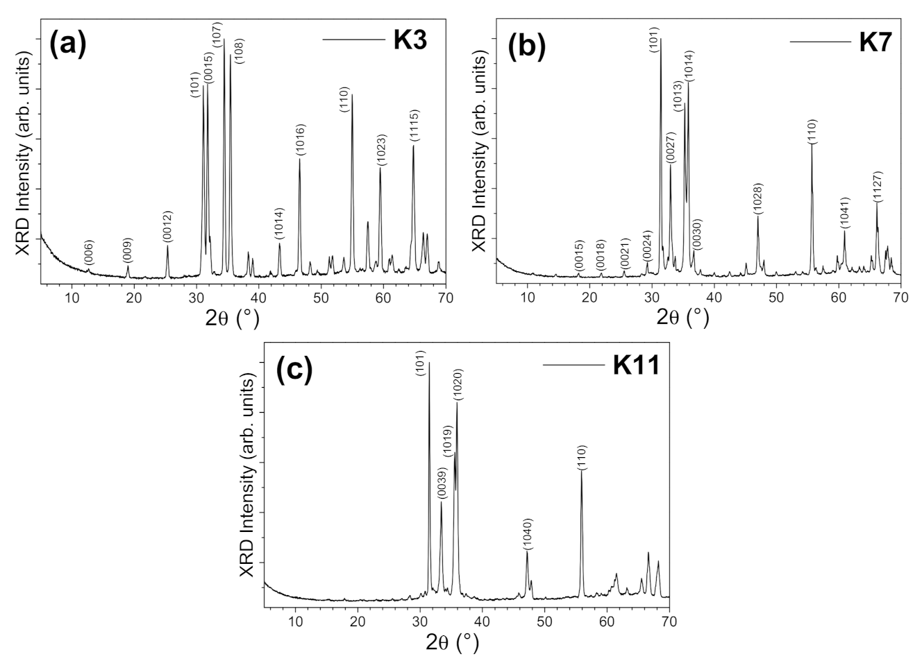
Figure 2a,c display the X-ray powder diffraction (XRD) patterns of the as-prepared samples Zn
3In
2O
6 (
k = 3), Zn
7In
2O
10 (
k = 7), and Zn
11In
2O
14 (
k = 11). All samples can be indexed on the basis of a
R-3
m space group and the obtained cell parameters for each term are collected in
Table 1, in agreement with previously reported data [
3,
7,
8].
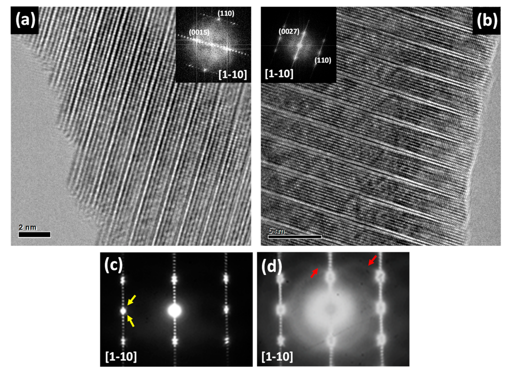
Figure 3a,b show representative conventional HRTEM images along the [1
0] zone axis and their corresponding Fast Fourier Transforms (FFT) (insets) of the terms
k = 3 and 7. Both images clearly show the formation of the superstructure and the stacking of the wurtzite blocks along the
c direction in a clearly ordered way. Although for
k = 3 a subtle variation in contrast is observed in the wurtzite block, this feature is unambiguously observed for
k = 7 as a dark zig-zag contrast inside the wurtzite block. As we discussed above, this contrast is attributed to the structural modulation formed by the inhomogeneous distribution of In
3+ in nanoclusters for terms
k ≥ 6 [
9,
10,
11]. This is confirmed by the presence of satellite reflections (marked with yellow arrows), which are clearly visualized in the corresponding SAED pattern (
Figure 3c) for the
k = 7 term. It is worth mentioning that, when the SAED pattern is recorded under high brightness and high exposure times (
Figure 3d), some diffuse lines (indicated by red arrows for better visualization) appear crossing the diffraction pattern, suggesting a structural order involving different wurtzite blocks.
At this point it is worth mentioning that, In3+ can diffuse under the electron beam making more challenging the interpretation of the experimental data. In order to assess the character of these extra inter-block order while assuring the integrity of the samples, the different IZO terms were investigated by low-dose (Cs)-corrected HRTEM by using a high sensitivity camera. In this sense, we studied the materials in milder working conditions in terms of radiation by the electron beam, avoiding the diffusion of In3+ cations that would result on non-real data.
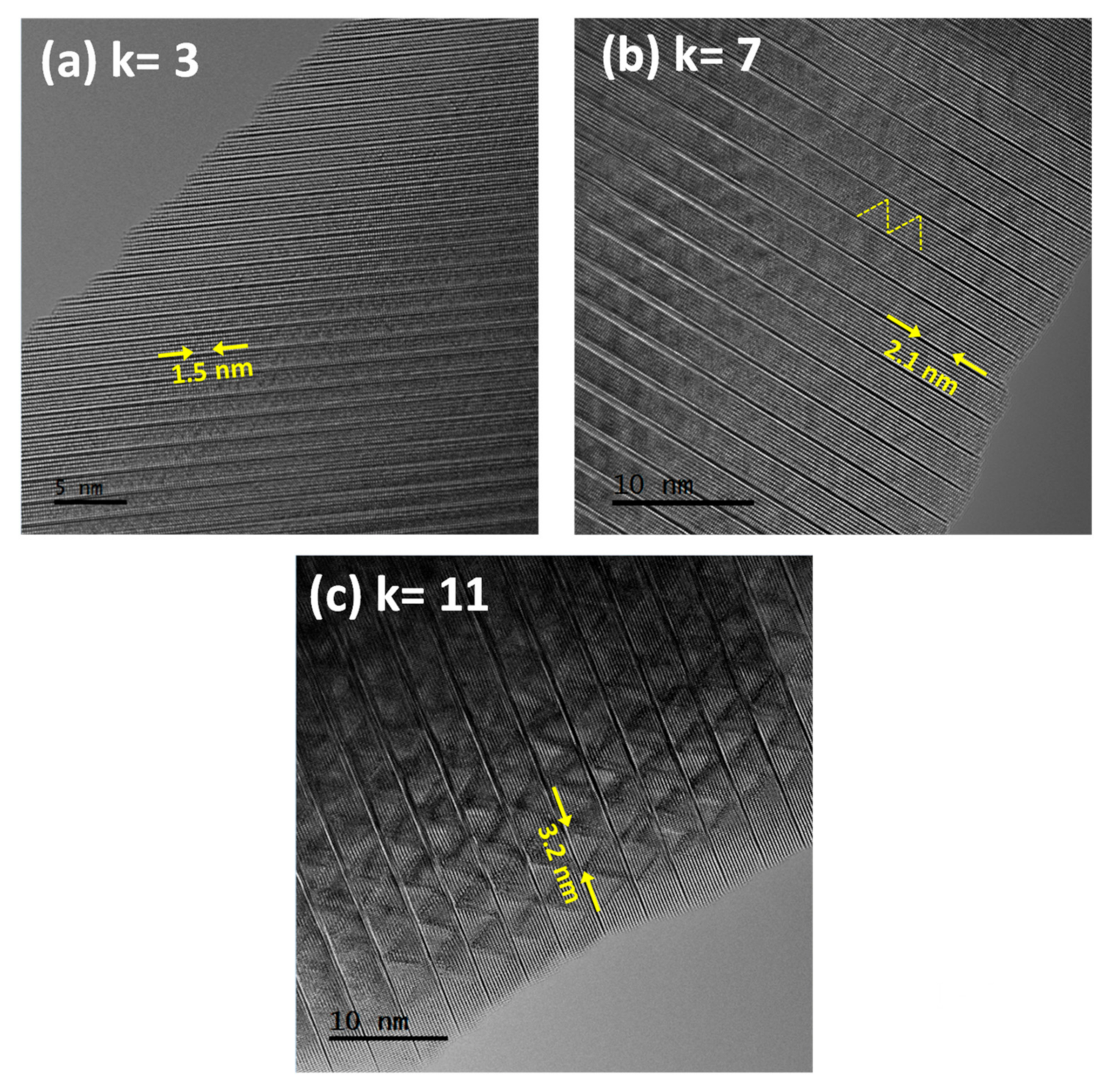
Figure 4a,c show the HRTEM images along the [1
0] direction for the three studied samples. The zig-zag contrast is identified within the wurtzite block. Notice that this contrast is also observed in the lowest term of the series (
k = 3), although the contrast of the zig-zag modulation is enhanced with increasing
k. This fact unambiguously confirms that the inhomogeneous distribution of In
3+ along the zig-zag planes is an inherent characteristic of all the terms of the homologous series as opposed to the generally accepted description that the modulation would only occur for terms with
k ≥ 6 [
9,
10,
11].
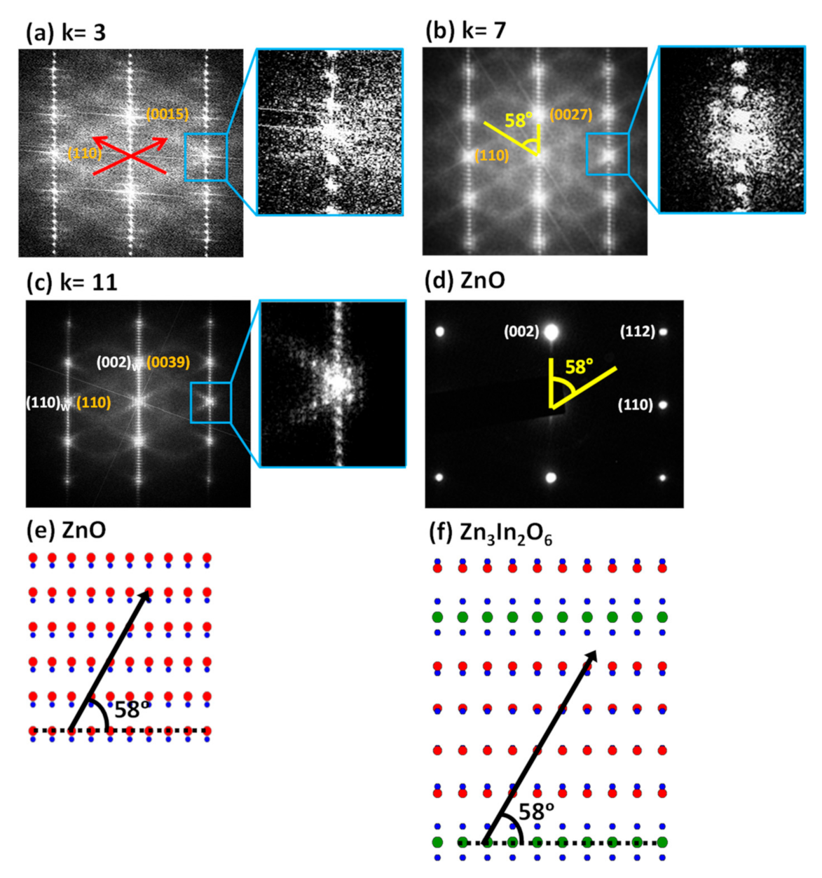
The corresponding FFTs of the described images are displayed in
Figure 5a–c. The presence of satellite reflections in all terms is confirmed (see the enlarged area around the (110) reflection) although, the definition of these maxima is consolidated for the higher
k terms, as expected. Note that the angle formed by satellite reflections and the (00
l) planes remains constant for all the terms with a value of 58°, revealing that the In
3+ is always distributed along the [112] direction of the ZnO wurtzite basic structure regardless of the thickness of the wurtzite-type In/Zn–O block in each term of the homologous series (
Figure 5d). Therefore, the In
3+ distribution within the wurtzite-type blocks seems to be independent of the
k value and, as a result, the period of the zig-zag modulation varies with
k, such that period values of 1.5, 2.1, and 3.2 nm were obtained for the terms
k = 3, 7, and 11, respectively (see
Figure 4).
The high sensibility of the camera also allowed us to detect, for all the samples, the presence of diffuse, but clearly directional, lines (marked, as example, with red lines in
Figure 5a) along the [112] direction of the wurtzite-basic structure, the same crystallographic directions observed for the zig-zag satellite spots. Therefore, the diffuse lines indicate that there is a short-range order correlation between the zig-zag planes of In
3+ along the different wurtzite blocks. Effectively, as it can be inferred from the images in
Figure 4, the In
3+ distribution is not perfectly ordered between the blocks, but shows a tendency to correlate along the [112] directions of the wurtzite-basic structure resulting in an inhomogeneous distribution of In
3+ nanoclusters in the structure. In the homologous series, this direction takes a different value for each term due to the different value of
l. Thus, it would be the [11
15] direction for the term
k = 3, [11
27] for
k = 7, and [11
39] for
k = 11. Therefore, the direction of these diffuse lines appears in a general way, along the [11
3k+6] direction for the odd
k terms and [11
2k+4] for the even
k terms. This difference has its origin in the different spatial groups used to describe the odd and even
k terms of the homologous series, as discussed earlier in the introduction. A schematic representation of ZnO and Zn
3In
2O
6 (
k = 3) along [1
0] is shown in
Figure 5e,f, respectively. In this representation, the ZnO [112] direction and the corresponding modulation direction in the term
k = 3, that is, the [11
15], have been indicated with black arrows, and are displayed together with the (00
l) planes in dashed lines and the 58° angle resulting from the intersection with the modulation direction.
It is important to note that the In/Zn ratio within the wurtzite block decreases as k increases, although the location of In3+ along the [112] wurtzite direction appears to be independent of the k value. In this sense, those terms with lower k values must accommodate more In3+ in a smaller number of atomic planes within the InZnkOk+1+ blocks as compared with the higher k terms. Therefore, it is expected that the In3+ located within the wurtzite-type blocks will result in distinct strain modulations for the different k terms of the homologous series.
In the following, we evaluate the deformation fields for the
k = 3 and
k = 7 terms, that is, below and above
k = 6, the term that has so far been recognised as the lowest in the Zn
kIn
2O
k+3 homologous series displaying the zig-zag structural modulation [
9,
10,
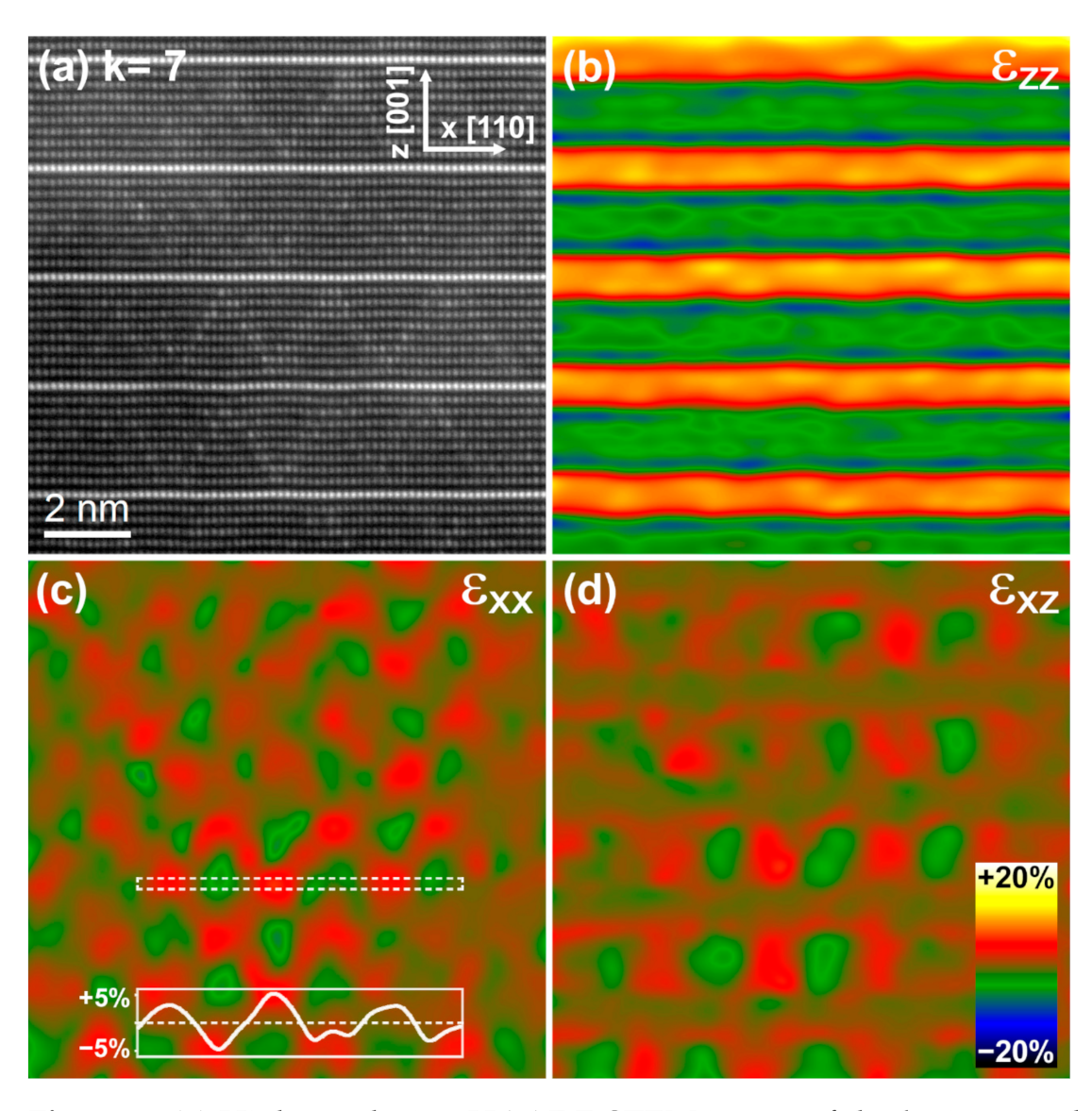
11]. For this purpose, HAADF-STEM images were obtained through aligning and averaging HAADF-STEM image series in order to correct for scan distortions, see
Figure 6a and
Figure 7a. Geometric Phase Analysis (GPA) [
24] was applied to measure the local deformations of the atomic lattice from the distortion-corrected HAADF-STEM images. The obtained local strain components are displayed as color-coded maps in
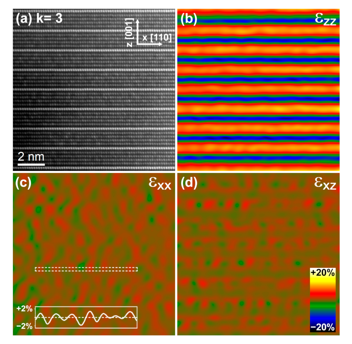
Figure 6b–d and
Figure 7b–d. As expected, the ε
zz strain component of
Figure 6b and
Figure 7b provides evidence for large lattice dilations along the [001] direction around the octahedral In–O layers. The dilation at these positions as compared to the wurtzite-type blocs is about 15 and 22% for the
k = 7 and 3, respectively. This observation is in good agreement with the
c lattice parameter values obtained by XRD. More interesting are, however, the strain features observed in the ε
xx strain map of
Figure 6c. Here, large dilations (in red) coincide with the In
3+ trigonal bipyramidal positions conforming the zig-zag structures present in the wurtzite-type blocks. Moreover, it is seen that the dilations are clearly larger at the apices of the zig-zag features than at the positions connecting neighboring apices. A line profile extracted along the white dashed box is shown as an inset in
Figure 6c. The dilatation strain at the apices of the zig-zag (in red) is up to 10% larger than at the center of the domains (in green). This value is more than twofold higher than the 4.5% value reported for the
k = 30 term [
25]. In
Figure 7c a similar strain pattern with maxima and minima is observed for the
k = 3 term. However, here the alternation of maxima and minima appears more disorganized and clear zig-zag features are only locally identified (see, e.g., the upper left corner). The line profile extracted along the white dashed box in
Figure 7c reveals that the strain difference between the (red) zig-zag apices and the (green) domains is about 3%, revealing a more homogeneous distribution of the In cations in the wurtzite-type layers than in the
k = 7 term. Finally, the ε
xz strain maps of both terms displayed in
Figure 6d and
Figure 7d exhibit very similar strain modulations further supporting the presence of a structural modulation in the
k = 3 term.
Interestingly, in
Figure 6a, subtle Zn/In atomic column displacements along the
c axis are clearly perceived when crossing the zig-zag features. These shifts were previously reported to be the result of a change in the orientation of the ZnO
4 tetrahedra on both sides of the zig-zags [
15,
19,
26]. Hence, the zig-zag features are inversion domains boundaries (IDBs) that separate adjacent domains of opposite polarity. We next investigated the inversion domain boundary distribution and the magnitude of the Zn/In atomic column displacements in the
k = 7 and 3 terms.
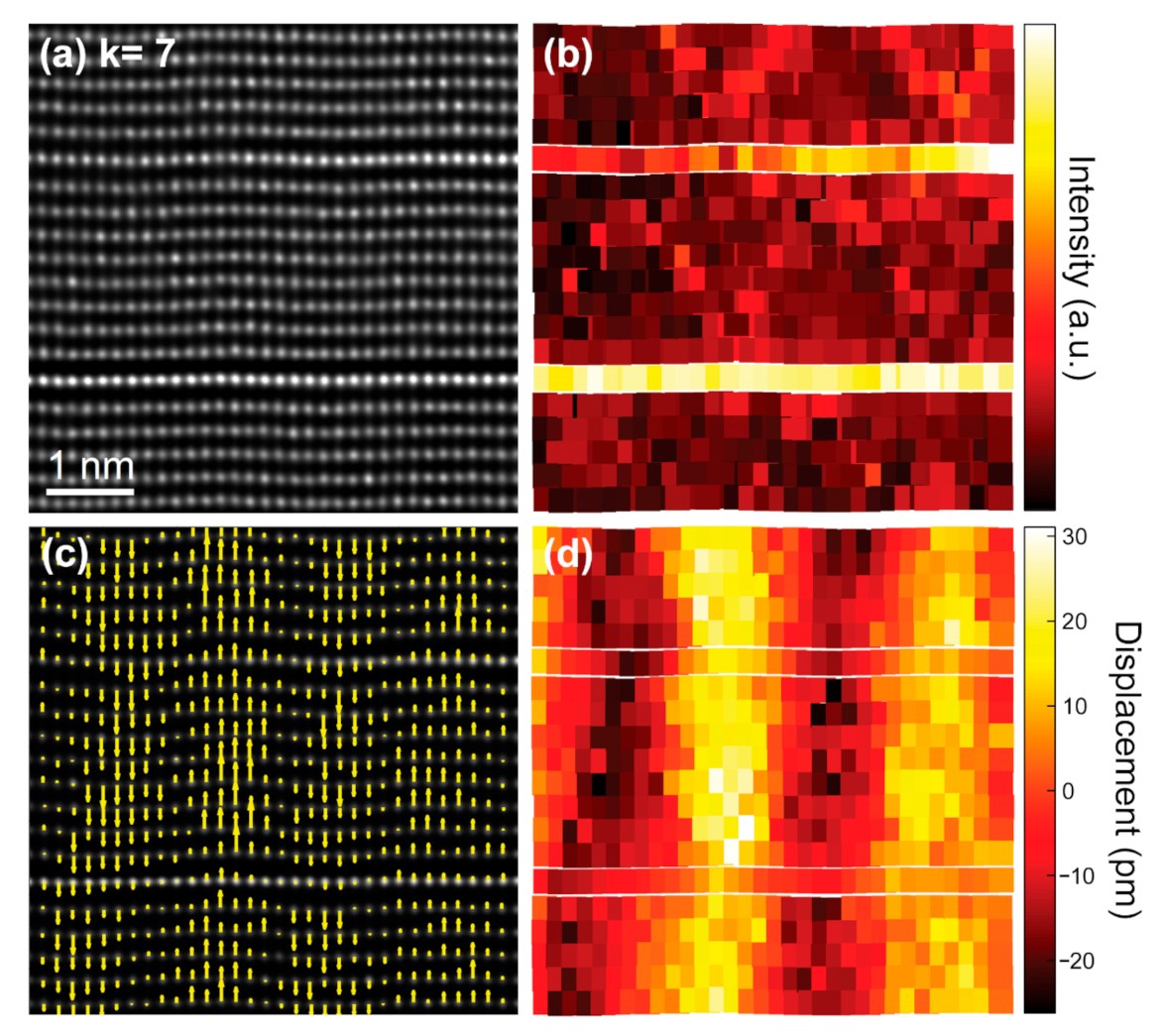
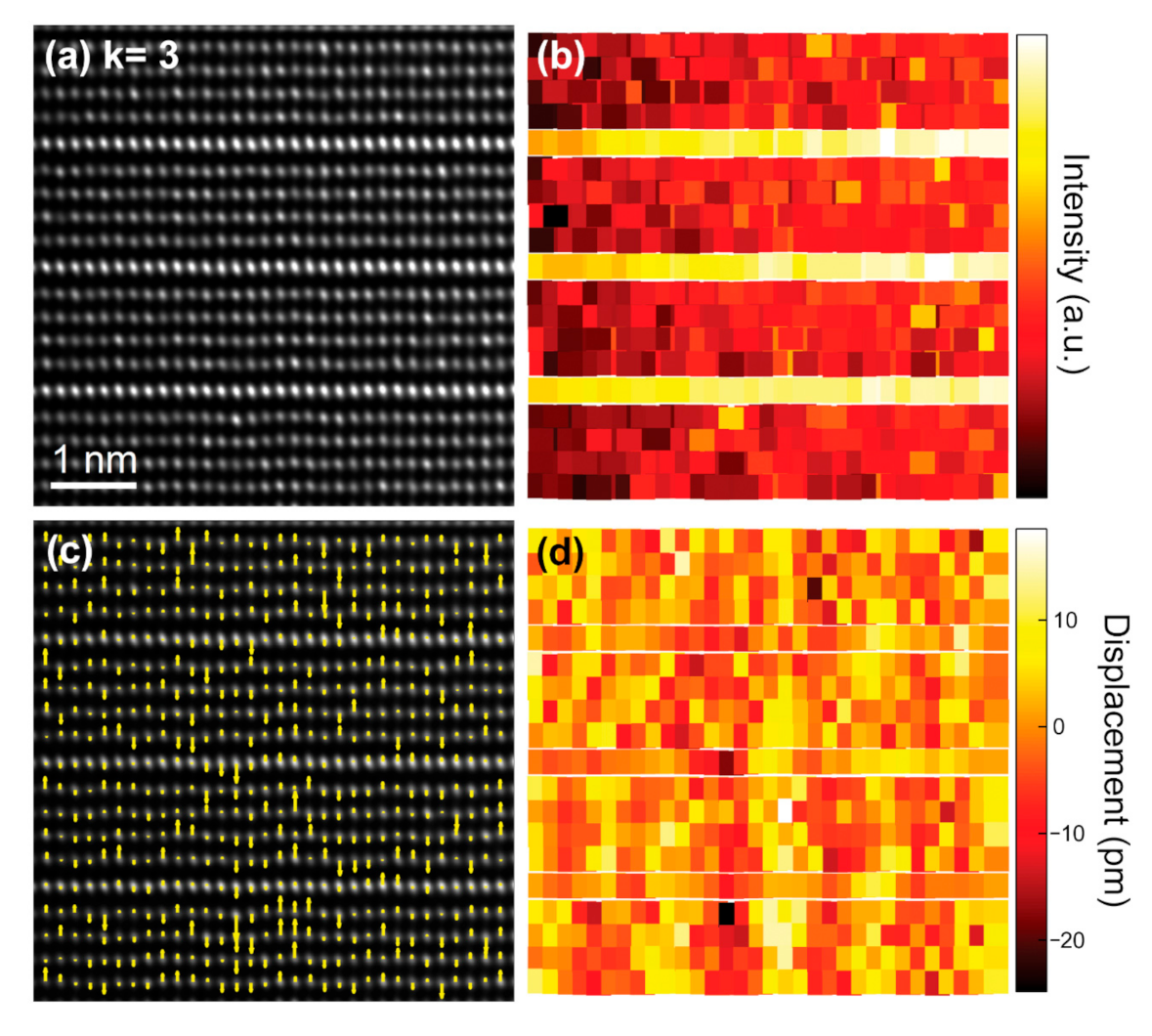
The positions of the atomic columns were directly determined on the deconvoluted images shown in
Figure 8a and
Figure 9a. Our fitting allows a quantitative estimation of the atomic column peak intensities and their positions with a precision of about 3 pm (see Materials and Methods section for details). The corresponding intensity maps of the metal sublattice are depicted in
Figure 8b and
Figure 9b. The zig-zag features are clearly visible with a brighter contrast in the intensity map of the
k = 7 term (
Figure 8b), but are only distinguishable in the lower left side of the intensity map of the
k = 3 term (
Figure 9b). Subsequently, the atomic displacements along the [001] direction of the Zn/In cations were measured relative to the center of each atomic row running along the [110] direction. The resulting vector maps are presented in
Figure 8c and
Figure 9c. The vectors in the arrow maps are plotted along the displacement direction of the Zn/In atomic columns, that is, away from the oxygen columns (not visible in the HAADF images). In both terms, it is evident that adjacent domains exhibit opposite polarity. As well, the Zn/In atomic column displacements are larger in the center of the domains and gradually diminish towards the IDBs.
Figure 8d and
Figure 9d are scattered color-code plots that give the magnitude of the Zn/In atomic column displacements in picometers. In the vicinity of the zig-zag apices, the measured atomic displacements are maximum; they are of the order of ±25 and ±13 pm for the
k = 7 and 3 terms, respectively.
Similarly to the strain analysis by GPA, the displacement analysis of the Zn/In atomic columns supports the occurrence of a zig-zag structural modulation in the
k = 3 term of the Zn
kIn
2O
k+3 homologous series. Nevertheless, compared to the
k = 7 term, in the
k = 3 term the modulation is less defined and only locally visible. This would explain the lower definition of the satellite reflections observed in the FFTs of
Figure 5a.
Considering the results shown above, an unambiguous nanodomain structure is identified for the ZnkIn2Ok+3 series whose origin is related with the zig-zag distribution of indium along the [113k+6] direction for the odd k terms and [112k+4] for the even k terms within the wurtzite block. The indium-induced structural distortion in the wurtzite block results in a change in the orientation of the ZnO4 tetrahedra on both sides of the indium planes (IDBs), giving rise to the nanodomain framework. The evaluation of atomically resolved vector maps also reveals that the nanodomains tend to correlate between different wurtzite-type blocks along the c direction, proving that the indium distribution has a significant effect on the entire structure of these materials. Interestingly, the indium distribution has revealed to be inherent to the homologous series, irrespective of the value of the k term. In this sense, a predictable behavior from the structural point of view can be expected for the ZnkIn2Ok+3 series in which a similar nanostructure framework must occur for all terms. Unfortunately, the fact of working with powdered samples rather than thin films, as well as the synthesis conditions (high temperature and long annealing times) could limit the potential use of these materials as TCOs. On the other hand, the possibility of perfectly controlling the In/Zn ratio from the k = 3 to the k = 11 expands the ability to tune the electro-optic functional response of the system, both characteristics confirming the high potential of IZOs for functional applications. The future work and perspectives of these phases would involve the development of new soft synthesis methods which allow the reduction of the particle size, and the possibility of integrating and growing these phases on substrates in a controlled way.

 ,
, 


