Two Types of Localized States in a Photonic Crystal Bounded by an Epsilon near Zero Nanocomposite


1
Institute of Nanotechnology, Spectroscopy and Quantum Chemistry, Siberian Federal University, 660041 Krasnoyarsk, Russia
2
Polytechnic Institute, Siberian Federal University, 660041 Krasnoyarsk, Russia
3
Institute of Engineering Physics and Radio Electronics, Siberian Federal University, 660041 Krasnoyarsk, Russia
4
Kirensky Institute of Physics, Federal Research Center KSC SB RAS, 660036 Krasnoyarsk, Russia
*
Author to whom correspondence should be addressed.
Photonics 2018, 5(3), 22; https://doi.org/10.3390/photonics5030022
Submission received: 5 July 2018
/
Revised: 24 July 2018
/
Accepted: 8 August 2018
/
Published: 9 August 2018
(This article belongs to the Special Issue Nonlinear Dielectric Photonics and Metasurfaces)
Abstract
:The spectral properties of a one-dimensional photonic crystal bounded by a resonant absorbing nanocomposite layer with the near-zero permittivity have been studied. The problem of calculating the transmittance, reflectance, and absorptance spectra of such structures at the normal and oblique incidence of light has been solved. It is shown that, depending on the permittivity sign near zero, the nanocomposite is characterized by either metallic or dielectric properties. The possibility of simultaneous formation of the Tamm plasmon polariton at the photonic crystal/metallic nanocomposite interface and the localized state similar to the defect mode with the field intensity maximum inside the dielectric nanocomposite layer is demonstrated. Specific features of field localization at the Tamm plasmon polariton and defect mode frequencies are analyzed.
1. Introduction
A special type of surface electromagnetic states in the form of a standing surface wave with the zero wavenumber along the interface between media, which does not transfer energy, have recently been in focus of researchers. In this case, the wave equation following from the Maxwell equations for an electric field is the exact analog of the one-electron Schrödinger equation for a semi-infinite crystal, the solution of which is the electronic Tamm state [1]. Therefore, the electromagnetic analog of the electronic Tamm state at the normal incidence of light onto a sample is called the optical Tamm state (OTS). If such a state exists at the interface between a photonic crystal (PhC) and a conducting medium with the effective permittivity < 0, the light wave interacts with a surface plasmon, i.e., the collective oscillation of the free electron gas at the conductor surface. The result of interaction between the radiation field and surface plasmon excitation is a Tamm plasmon polariton (TPP) [2], which is observed in experiments as a narrow peak in the energy spectra of a sample [3,4,5]. As was shown in [6,7,8,9,10], the materials with the negative permittivity ( < 0) adjacent to a PhC can be both metallic films and nanocomposites with the resonant frequency dispersion.
Theoretical and experimental investigations of the properties of TPPs allowed them to be used as the basis of a fundamentally new class of devices, including absorbers [11,12,13,14], switchers [15], organic solar cells [16], thermal emitters [17,18], sensors [19,20,21], and spontaneous radiation amplifiers [22]. The high degree of field localization at the TPP frequency makes it possible to reduce the threshold of generation of nonlinear effects [23,24,25] and implement the extremely high light transmission through a nanohole [26]. The interaction of the TPPs with other types of localized modes allows lasers [27,28], induced transparency [29], single-photon sources [30], and electro-optically tunable Tamm plasmon-polariton-excitons [31] to be obtained. In [32,33], we found the localized state in the structure containing a cholesteric liquid crystal. Later, a chiral analog of the TPP in a cholesteric liquid crystal was established [34]. In this case, the polarization-preserving anisotropic mirror made of a metal-dielectric nanocomposite was used as a metallic layer [35].
Of great interest are materials with the near-zero permittivity. Such structures are used to control the wave front shape [36]; enhance the transmission of light through a subwavelength aperture [37] and nonlinear effects [38,39]; develop absorbers [40], photonic wires [41], and insulators [42]; and perform the third-harmonic generation [43]. The materials with the near-zero permittivity involve layered plasmon structures, indium tin oxide (ITO), metal-dielectric, polymer nanocomposites, and composites with core–shell nanoparticles. In this work, we demonstrate the possibility of simultaneous implementation of the TPP and defect mode localized at the interface between a PhC and a nanocomposite with the near-zero effective permittivity [44]. The nanocomposite consists of metallic nanoparticles dispersed in a transparent matrix and has the resonant effective permittivity. The optical characteristics of initial materials have no resonant features [45,46,47]. The position of a frequency band corresponding to the near-zero effective permittivity is determined by the permittivities of initial materials and volume concentration of nanoparticles. This opens wide opportunities for guiding the optical properties of localized states.
2. Model Description and Determining the Transmittance
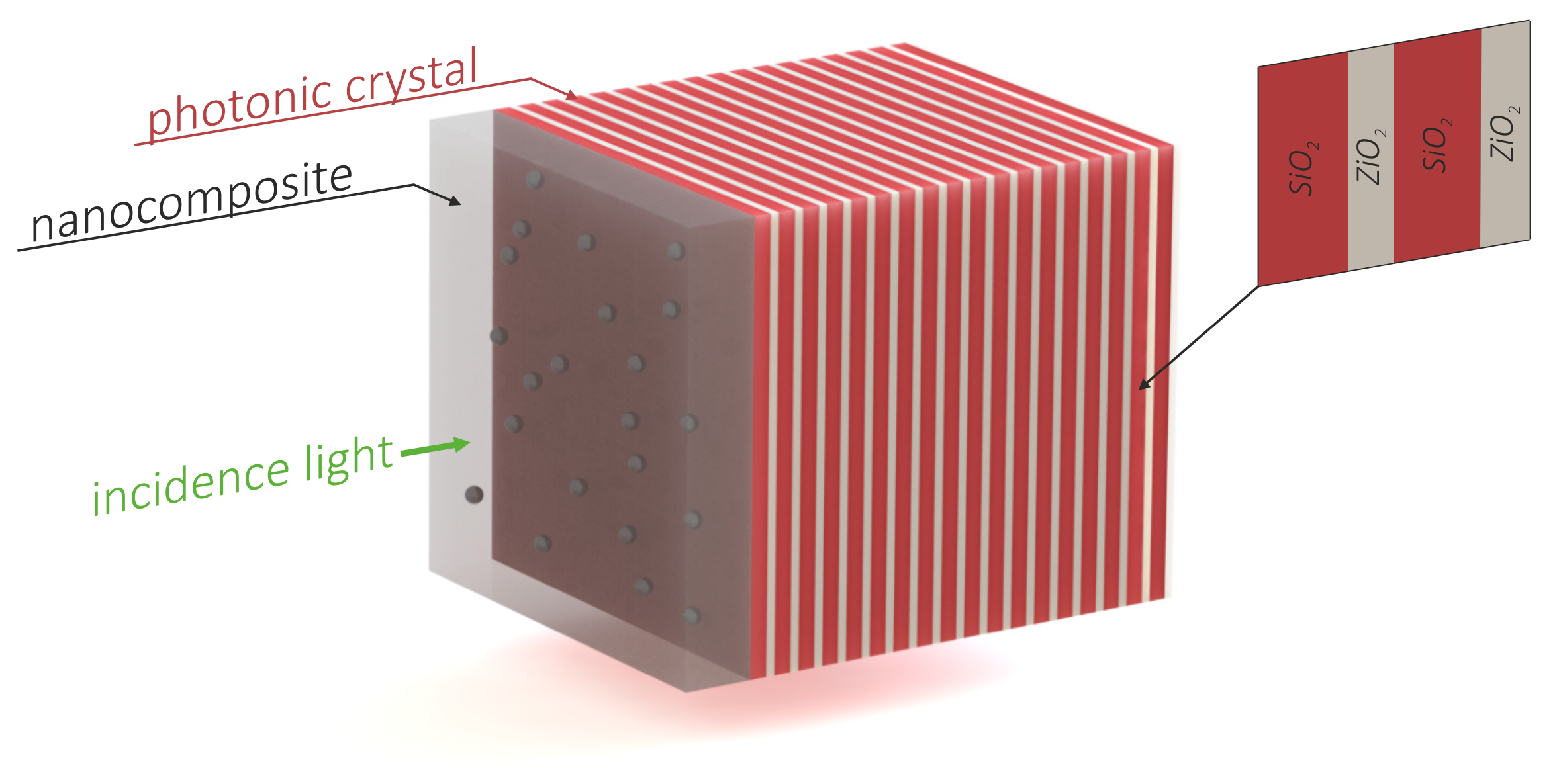
We consider a PhC structure in the form of a layered medium bounded by a nanocomposite layer with finite thickness (Figure 1). The PhC unit cell is formed of materials a and b with respective layer thicknesses and and permittivities and .
The nanocomposite layer with thickness consists of spherical metallic nanoparticles uniformly distributed in a dielectric matrix.
Hereinafter, we assume the PhC structure to be placed in vacuum.
The effective permittivity of the nanocomposite is determined using the Maxwell Garnett formula [48,49] widely used in studying matrix media, in which isolated metallic inclusions with a small volume fraction are dispersed in the matrix material
where f is the filling factor, i.e., the fraction of nanoparticles in the matrix; and () are the permittivities of the matrix glass and nanoparticle metal, respectively; and is the radiation frequency.
The Maxwell Garnett model suggests the quasi-steady-state approximation. The model has the following specific features: the nanocomposite layer is electrodynamically isotropic and the size of inclusions and distance between them are much smaller than the optical wavelength in the investigated effective medium. We determine the permittivity of a nanoparticle metal using the Drude approximation
where is the constant taking into account the contributions of interband transitions of bound electrons; is the plasma frequency; and is the reciprocal electron relaxation time.
The change in the light field upon its passing through each structural layer is determined by the transfer matrix method [50].
3. Results and Discussion
We investigate the localized states formed at the PhC/nanocomposite interface. The nanocomposite consists of metallic nanospheres dispersed in a dielectric matrix and is characterized by the resonant effective permittivity
In approximation , it follows from Equation (1) that the real part of the effective permittivity at nonzero f takes the zero value at two points with the frequencies
In the range of (, ), the nanocomposite is similar to the metal. It means that, in this frequency range, the TPP can exist at the PhC/nanocomposite interface. At , the nanocomposite plays the role of a dielectric layer with and and, as we show below, the localized (defect) mode with the electric field intensity maximum inside the layer can exist along with the TPP.
In our structure, the materials of alternating PhC layers are silicon dioxide (SiO) with a permittivity of and zirconium dioxide (ZrO) with a permittivity of . The respective layer thicknesses are nm and nm and the number of layers is .
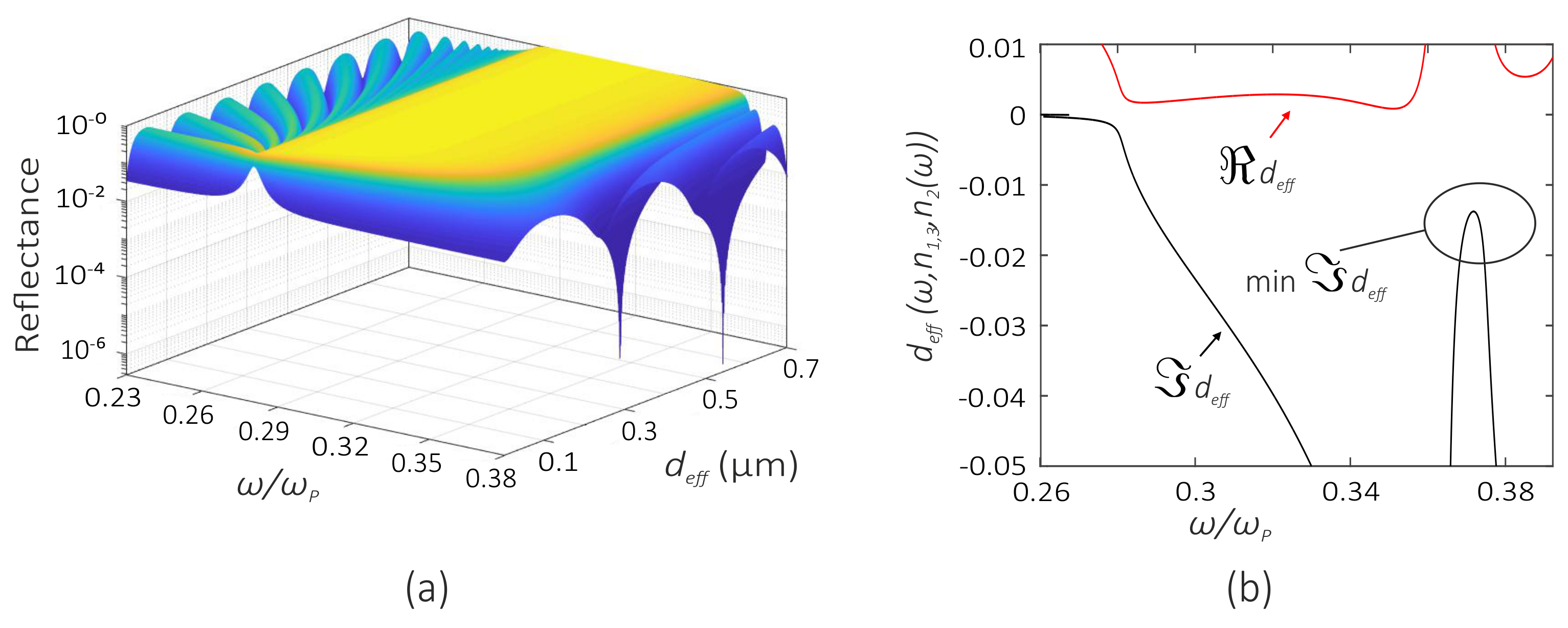
The epsilon near zero nanocomposite layer with a thickness of nm consists of silver nanospheres dispersed in transparent optical glass. The parameters of silver are , eV, and eV and the permittivity of glass is . The frequency dependences of the real and imaginary parts of permittivity calculated using Equation (1) show that, as the volume concentration of the nanospheres in the nanocomposite film increases, the frequency corresponding to the collective plasmon resonance shifts to the low-frequency region. In this case, the half-width of the resonance curve changes insignificantly, the curve is noticeably modified, and the frequency range corresponding to broadens out. As an example, Figure 2 shows the and curves at , together with the transmittance, reflectance, and absorbance spectra of a PhC conjugated with a nanocomposite film. The PhC band gap is limited by a frequency range of 0.26 .
It can be seen in Figure 2 that near the high-frequency boundary of the PhC band gap, the absorption bands arise, which correspond to the localized states formed at the PhC/nanocomposite interface. The low-frequency state with ( nm) exists in the range with < 0 (TPP) and the high-frequency state with ( nm), in the range with (defect mode). At the TPP frequency, the effective permittivity takes the values of and, at the defect mode frequency, .
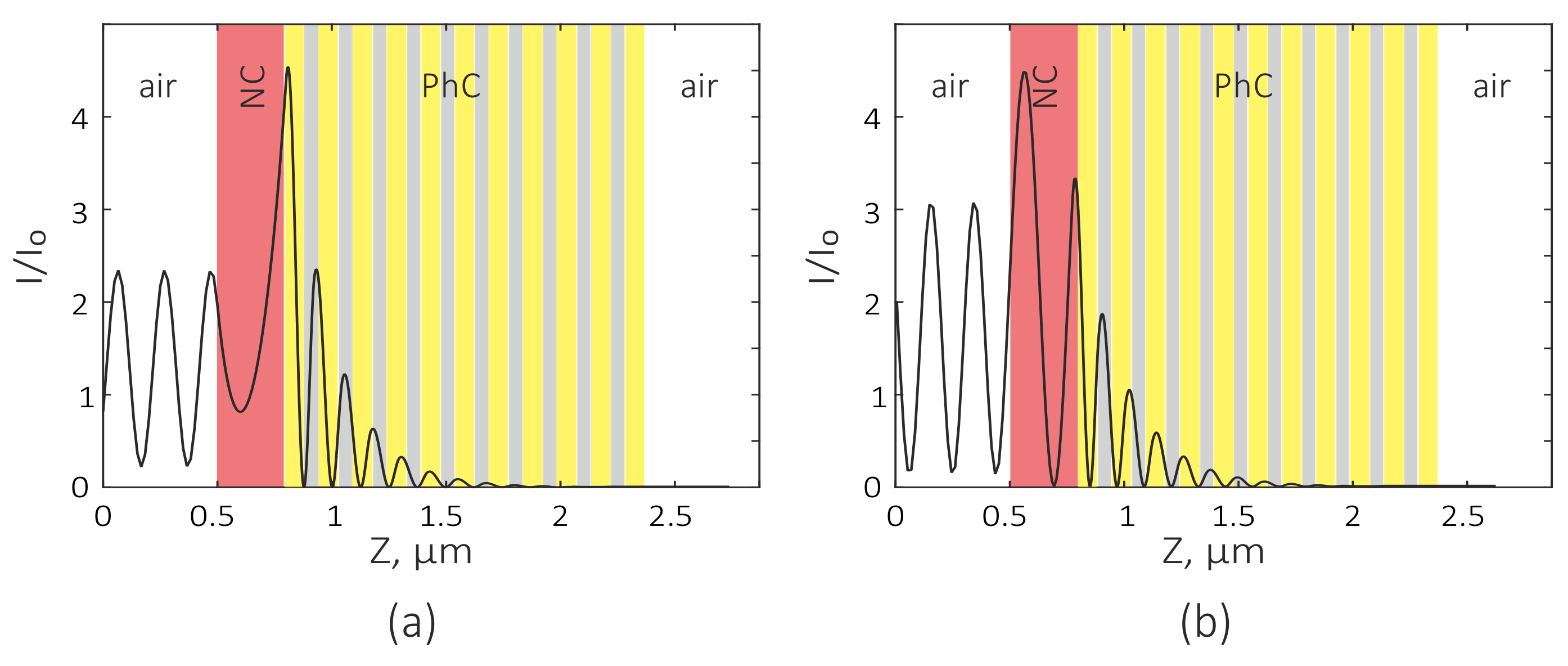
The electric field intensity distribution at the corresponding frequencies of the localized states at the contact between the PhC and nanocomposite film is illustrated in Figure 3.
It can be seen in Figure 3 that, for the TPP, the field is localized at the PhC/nanocomposite interface and, for the defect mode, in the bulk of the nanocomposite layer.
The localization values are almost the same. In both cases, the light field in the states is localized in the region comparable with the wavelength.
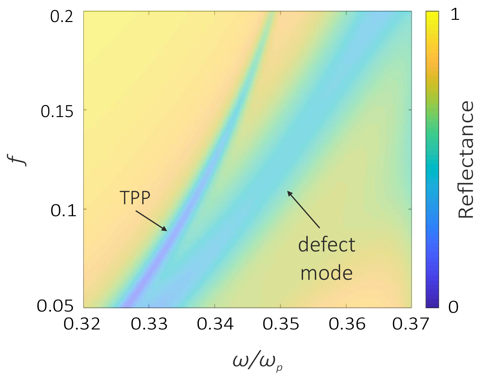
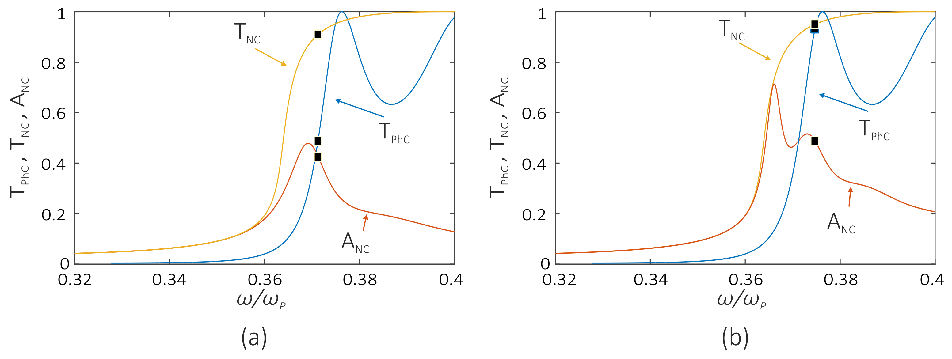
The change in the nanocomposite filling factor is a powerful tool for frequency tuning. The reflectance spectra of the investigated structure calculated at different nanocomposite filling factors are shown in Figure 4.
It can be seen in Figure 4 that the increase in the volume concentration of metallic inclusions in the bulk of nanocomposite leads to the shift of localized states to the high-frequency region. In this case, the frequency range between the TPP and defect mode reflection minima also increases. Note that with an increase in the filing factor, the reflectance at the TPP frequency increases. According to the energy conservation law, the absorption in the nanocomposite layer decreases and can be controlled by changing the layer thickness.
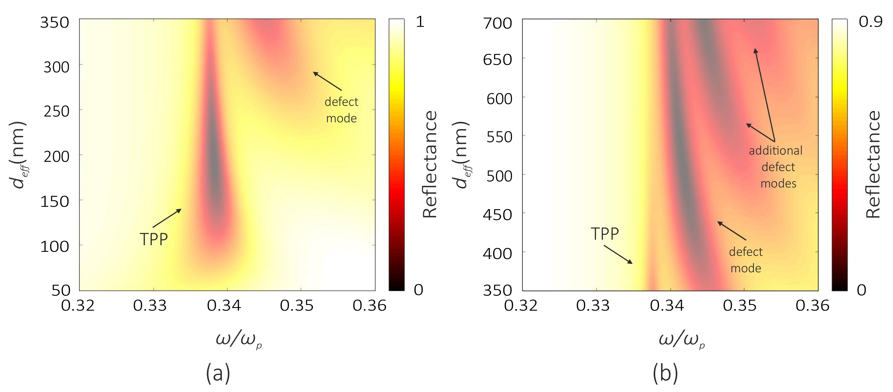
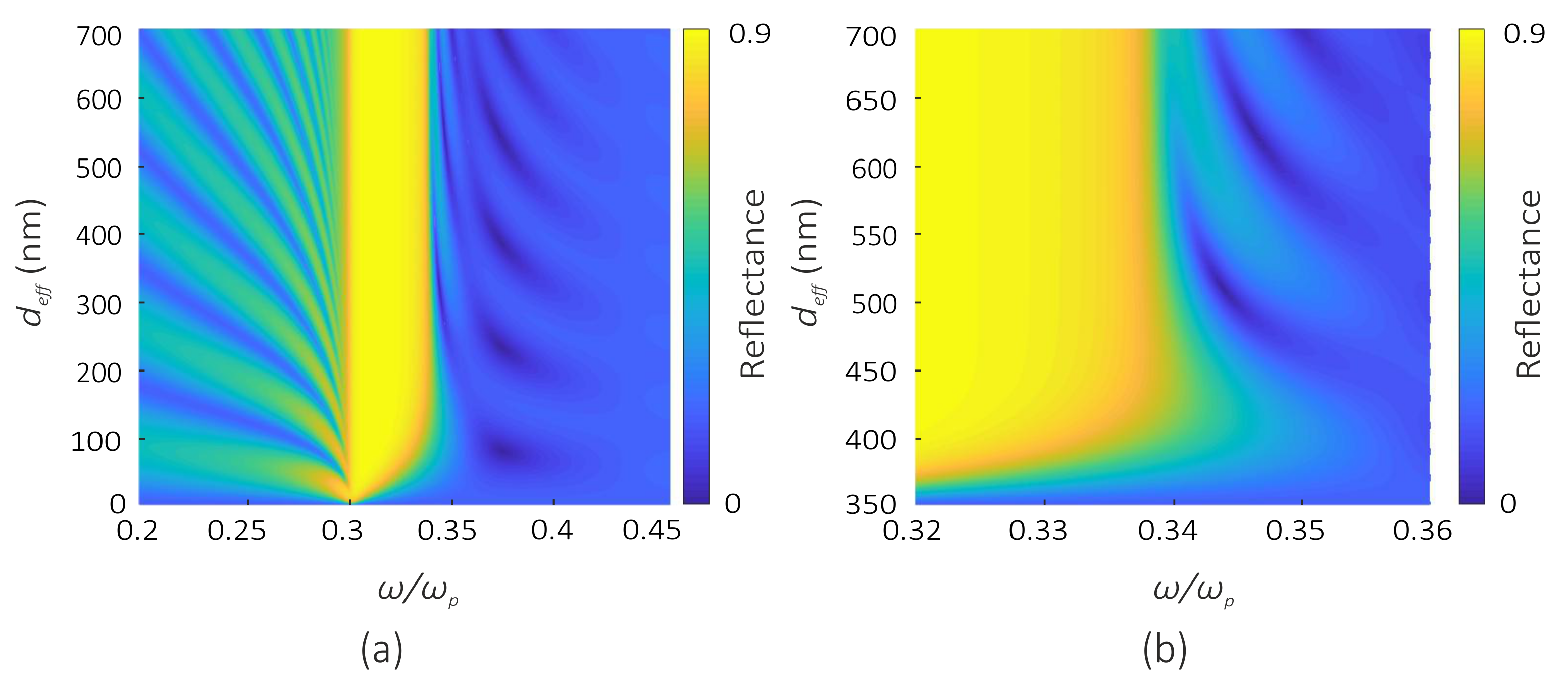
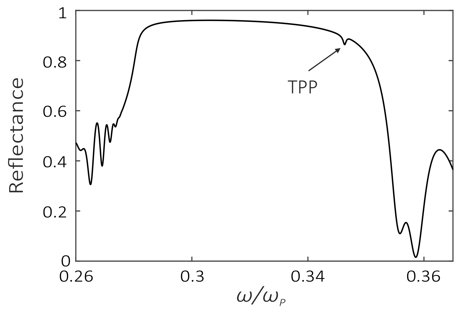
Reflectance spectra of the PhC/nanocomposite structure with different nanocomposite film thicknesses are presented in Figure 5.
The change in the nanocomposite layer thickness leads to the significant variation in the reflectance spectrum in the frequency range near . In particular, in the nanocomposite film with a thickness of up to 250 nm, only the TPP exists. The reflectance minimum is observed at a thickness of nm (Figure 5a). The use of nanocomposite films thicker than 250 nm leads to the formation of a defect mode and corresponding second reflectance gap. At the same time, the second and third orders of defect modes are formed at thicknesses greater than 450 nm and 650 nm, respectively. The second reflectance minimum corresponds to a thickness of nm. It should be noted that, at nm, the TPP does not exist (Figure 5b).
The calculations show that the defect mode is an eigenmode of the Fabry–Pérot dielectric resonator, which is represented by a nanocomposite enclosed between the PhC and the vacuum half-space. For such a resonator, we can write
where N is the mode number.
At a frequency of and a permittivity of , the wavelength is nm in vacuum and, according to Equation (5), nm in the nanocomposite layer; therefore, the thickness nm corresponds to half-wavelength condition Equation (5).
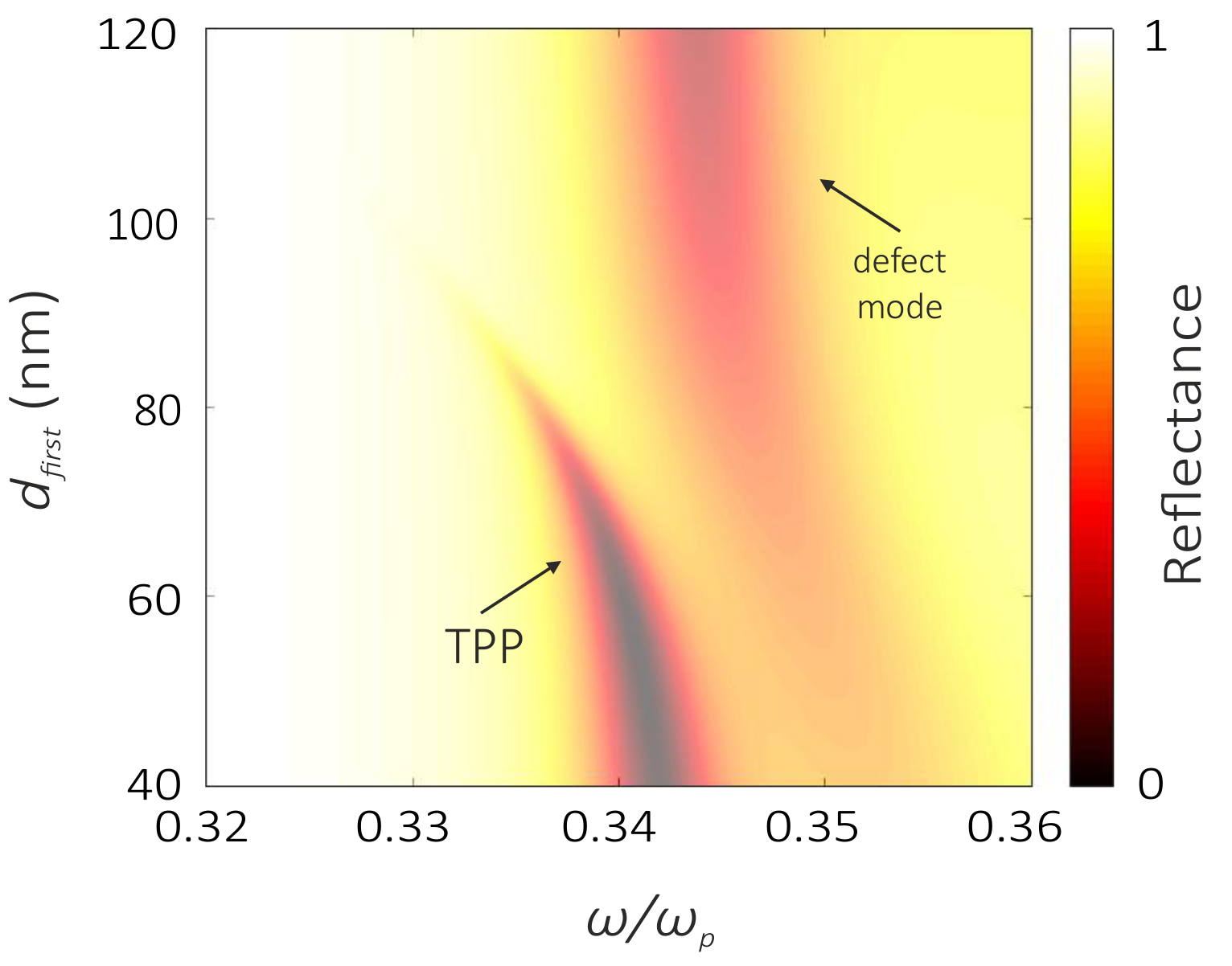
Figure 6 shows reflectance spectra of the structure in dependence of PhC first-layer thickness . The thickness variation can be ensured by forming a sharp-wedge-shaped layer [51]. In this case, an insignificant destruction of plane-parallelism of the layers can be compensated by a correct choice of the optical beam width.
It can be seen in Figure 6 that the frequency positions of the localized states and distance between them significantly change upon variation in the first-layer thickness . The increase in leads to the shift of the TPP and defect mode frequencies toward longer wavelengths. This avoided crossing is a common signature of mode coupling. In this case, a sort of switching between the TPP and defect mode is implemented. It can be seen that the defect mode exists when the first-layer thickness is larger than 85 nm; in this case, the TPP does not exist.
Such a switching from the TPP to defect mode upon variation in the PhC first-layer thickness makes these structures promising for application in tunable filters and sensors.
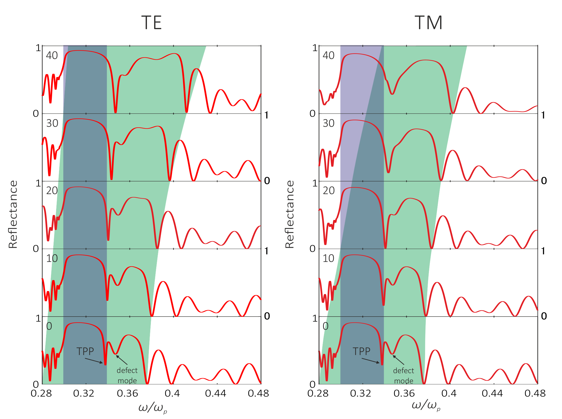
Along with the aforesaid, one of the effective ways of controlling the energy spectra is changing the angle of incidence of light onto a sample. Study of the reflectance spectra showed that for the TE modes the increase in the angle of incidence leads to the broadening of the initial PhC band gap and its shift to the high-frequency range (Figure 7).
It is noteworthy that the overlap of the region with and the band gap is observed over the entire range of investigated angles. However, the TPP does not exist at angles over 30 degrees. This is due to the fact that the increase in the angle of incidence leads to the TPP shift to the high-frequency region, crossing the point , and TPP transformation to the defect mode.
The different picture is observed for the TM waves. The increase in the angle of incidence leads to the stronger shift of the PhC band gap to the high-frequency region than in the case of TE modes. At angles more than 40 degrees, the region with and PhC band gap stop overlapping. In this case, the TPP does not exist, as for the TE modes, at angles over 30 degrees.
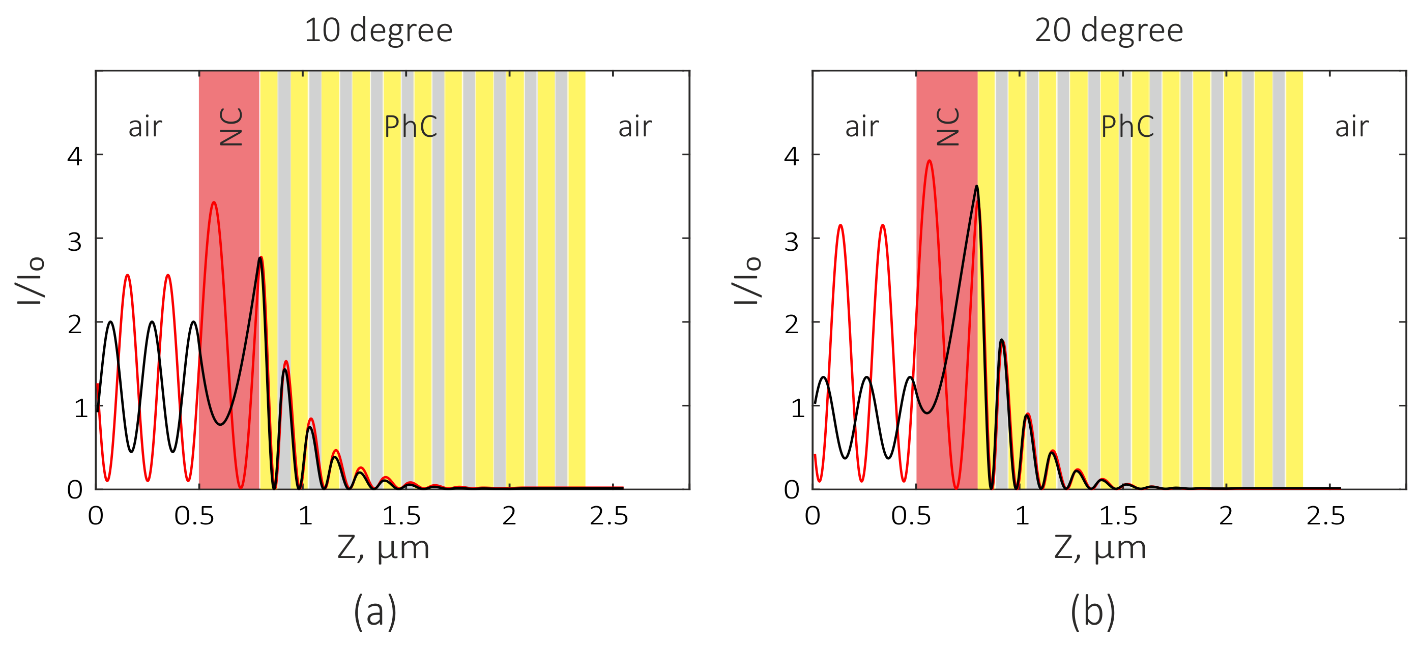
The electric field intensity distribution at oblique light incidence on the structure is illustrated in Figure 8.
Analysis of Figure 8 shows that the field distribution is analogous to the case of normal incidence (Figure 3). It should be noted that the overlapping spatial distributions of the field do not help in determining the mode coupling. In this case, the mode coupling can be established through transmission or reflection spectra by mean of changing of the first layer thickness (Figure 6).
3.1. Fresnel Reflection from a Nanocomposite Film
Let us clarify the nature of formation of the localized states at the small negative and positive nanocomposite permittivities. We calculate the Fresnel reflectance from the nanocomposite film with finite thickness [52].
The reflectances at the first and second film boundaries are
where and are the refractive indices of the air and silicon dioxide, respectively, . The total reflectance is determined as:
where , and is the nanocomposite film thickness.
Figure 9 shows the calculated dependence of the Fresnel reflectance on the nanocomposite layer thickness at the normal incidence of light onto the nanocomposite.
It can be seen in Figure 9a that, at a nanocomposite film thickness of 300 nm at the TPP frequency (), the Fresnel reflectance from the nanocomposite attains 58%, which facilitates the localized state formation at the PhC/nanocomposite interface. At the same nanocomposite film thickness at a defect mode frequency , the reflectance is about 5%.
At the local intensity of the field at the TPP frequency decreases. Contrariwise, at the defect mode frequency, it increases. The reflection zero condition can be written in account of Equation (7):
Using this equations, we can express ; this is a complex quantity, which will have the form
Equation (8) can be built numerically or graphically; then, the number of varied parameters will increase to three, since, along with the variation in the incident radiation frequency and nanocomposite layer thickness, we can change the nanocomposite filling factor. This allows us to solve Equation (8) at zero reflectance (Equation (7)) at the frequencies corresponding to the near-zero effective permittivity of the nanocomposite. It was established that this condition is satisfied at % (Figure 10).
It can be seen in Figure 10a that, in the investigated nanocomposite layer thickness range, there are two solutions at frequencies of and . In this case, and 576 nm, respectively.
It should be noted that, in this case, the condition in Equation (5) is also met, since, at a frequency of and , the wavelength is nm in vacuum and nm in the nanocomposite layer; therefore, the thickness nm is almost consistent with the half-wavelength condition ( in Equation (5)). At a frequency of and , the wavelength is nm in vacuum and nm in the nanocomposite layer. Thus, the thickness nm is almost consistent with the wavelength in the medium ( in Equation (5)).
3.2. Coupled Mode Theory
The principle of defect mode formation can be explained using the coupled mode theory. According to this theory, the defect mode formation involves the contributions of three energy channels, each characterized by relaxation rate . The relaxation rate is equal to the ratio between the total power of energy relaxation and the energy accumulated in the defect mode. We denote the rates of energy relaxation to the transmission and absorption channels of the nanocomposite film and the transmission channel of the PhC by , , and , respectively. The energy accumulated in the defect layer is the same for determining the rate of relaxation to each channel. Therefore, the ratio between relaxation rates is determined by the ratio between powers of leakage to the channels and can be related to the energy coefficients of the structure as [18]:
In this case, the energy accumulated in the defect mode will be maximal under the critical coupling condition
The graphic verification of the validity of critical coupling conditions (10) at nanocomposite layer thicknesses of and 576 nm is illustrated in Figure 11.
Note that, at a wavelength of nm, the condition in Equation (10) is valid, while at nm, it is invalid. This can be explained by the low Q factor of the resonator mode at nm. In this case, the coupled mode theory allows the process to be only qualitatively, yet not quantitatively, described [53].
To check the validity of the critical coupling conditions for the TPP in the case of a PhC conjugated with the 341-nm thick nanocomposite, we write the expression analogous to Equation (10):
Analysis of the energy spectra of the structure showed that at the TPP from the nanocomposite film side, the condition in Equation (11) is not met because of the weak coupling of the incident radiation with the TPP (Figure 12).
However, the coupled mode theory makes it possible to estimate the reflectance value relative to the background radiation at the frequency of the TPP excited from the nanocomposite side:
The transfer-matrix results and coupled mode theory data are given in Table 1.
Thus, the coupled mode theory gives a good agreement with the transfer matrix method.
4. Conclusions
We examined the spectral properties of a one-dimensional photonic crystal conjugated with the resonant absorbing nanocomposite layer consisting of spherical silver nanoparticles dispersed in transparent optical glass. We showed first that, in the frequency band where the effective permittivity takes near-zero values, the nanocomposite exhibits the properties of both a metal and a dissipative dielectric. As a result, both the Tamm plasmon polariton and defect mode exist at the photonic crystal/nanocomposite interface. We demonstrated that the field localization at the Tamm plasmon polariton and defect mode can be the same. We established the nanocomposite film thicknesses at which both modes can simultaneously exist in the structure. We showed that the frequency positions of the modes can be effectively controlled by varying the thickness of a photonic crystal layer adjacent to the nanocomposite and the nanocomposite filling factor. The obtained results scale up possible implementations of Tamm plasmon polaritons in resonant photonic crystal structures.
Author Contributions
R.G.B. performed the calculations, visualized the results and drafted the manuscript. I.V.T. helped with software, methods and checked analytical expressions, S.Y.V. supervised the whole study and finalized the manuscript.
Funding
This research was funded by RFBR according to the research projects No. 18-32-00053 and by Russian Foundation for Basic Research, Government of Krasnoyarsk Territory, Krasnoyarsk Region Science and Technology Support Fund to the research project No. 17-42-240464.
Conflicts of Interest
The authors declare no conflict of interest.
References
- Tamm, I.E. On the possible bound states of electrons on a crystal surface. Phys. Z. Sowjetunion 1932, 1, 733–735. [Google Scholar]
- Kaliteevski, M.A.; Iorsh, I.; Brand, S.; Abram, R.A.; Chamberlain, J.M.; Kavokin, A.V.; Shelykh, I.A. Tamm plasmon-polaritons: Possible electromagnetic states at the interface of a metal and a dielectric Bragg mirror. Phys. Rev. B 2007, 76, 165415. [Google Scholar] [CrossRef] [Green Version]
- Goto, T.; Dorofeenko, A.V.; Merzlikin, A.M.; Baryshev, A.V.; Vinogradov, A.P.; Inoue, M.; Lisyansky, A.A.; Granovsky, A.B. Optical tamm states in one-dimensional magnetophotonic structures. Phys. Rev. Lett. 2008, 101, 14–16. [Google Scholar] [CrossRef] [PubMed]
- Sasin, M.E.; Seisyan, R.P.; Kaliteevski, M.A.; Brand, S.; Abram, R.A.; Chamberlain, J.M.; Egorov, A.Y.; Vasil’ev, A.P.; Mikhrin, V.S.; Kavokin, A.V. Tamm plasmon polaritons: Slow and spatially compact light. Appl. Phys. Lett. 2008, 92, 251112. [Google Scholar] [CrossRef] [Green Version]
- Sasin, M.E.; Seisyan, R.P.; Kaliteevski, M.A.; Brand, S.; Abram, R.A.; Chamberlain, J.M.; Iorsh, I.V.; Shelykh, I.A.; Egorov, A.Y.; Vasil’ev, A.P.; et al. Tamm plasmon-polaritons: First experimental observation. Superlatt. Microstruc. 2010, 47, 44–49. [Google Scholar] [CrossRef]
- Vetrov, S.Y.; Bikbaev, R.G.; Timofeev, I. Optical Tamm states at the interface between a photonic crystal and a nanocomposite with resonance dispersion. J. Exp. Theor. Phys. 2013, 117, 988–998. [Google Scholar] [CrossRef]
- Vetrov, S.Y.; Bikbaev, R.G.; Timofeev, I. The optical Tamm states at the edges of a photonic crystal bounded by one or two layers of a strongly anisotropic nanocomposite. Opt. Commun. 2017, 395, 275–281. [Google Scholar] [CrossRef] [Green Version]
- Vetrov, S.Y.; Pankin, P.S.; Timofeev, I. The optical Tamm states at the interface between a photonic crystal and a nanocomposite containing core–shell particles. J. Opt. 2016, 18, 065106. [Google Scholar] [CrossRef] [Green Version]
- Bikbaev, R.G.; Vetrov, S.Y.; Timofeev, I. The optical Tamm states at the interface between a photonic crystal and nanoporous silver. J. Opt. 2017, 19, 015104. [Google Scholar] [CrossRef]
- Bikbaev, R.G.; Vetrov, S.Y.; Timofeev, I. Optical Tamm states at the interface between a photonic crystal and a gyroid layer. J. Opt. Soc. Am. B 2017, 34, 2198–2202. [Google Scholar] [CrossRef]
- Gong, Y.; Liu, X.; Wang, L.; Lu, H.; Wang, G. Multiple responses of TPP-assisted near-perfect absorption in metal/Fibonacci quasiperiodic photonic crystal. Opt. Express 2011, 19, 9759–9769. [Google Scholar] [CrossRef] [PubMed]
- Gong, Y.; Liu, X.; Lu, H.; Wang, L.; Wang, G. Perfect absorber supported by optical Tamm states in plasmonic waveguide. Opt. Express 2011, 19, 18393–18398. [Google Scholar] [CrossRef] [PubMed]
- Fang, M.; Shi, F.; Chen, Y. Unidirectional All-Optical Absorption Switch Based on Optical Tamm State in Nonlinear Plasmonic Waveguide. Plasmonics 2016, 11, 197–203. [Google Scholar] [CrossRef]
- Xue, C.H.; Wu, F.; Jiang, H.T.; Li, Y.; Zhang, Y.W.; Chen, H. Wide-angle Spectrally Selective Perfect Absorber by Utilizing Dispersionless Tamm Plasmon Polaritons. Sci. Rep. 2016, 6, 39418. [Google Scholar] [CrossRef] [PubMed] [Green Version]
- Zhang, W.; Yu, S. Bistable switching using an optical Tamm cavity with a Kerr medium. Opt. Commun. 2010, 283, 2622–2626. [Google Scholar] [CrossRef]
- Zhang, X.L.; Song, J.F.; Li, X.B.; Feng, J.; Sun, H.B. Optical Tamm states enhanced broad-band absorption of organic solar cells. Appl. Phys. Lett. 2012, 101, 243901. [Google Scholar] [CrossRef]
- Yang, Z.Y.; Ishii, S.; Yokoyama, T.; Dao, T.D.; Sun, M.G.; Nagao, T.; Chen, K.P. Tamm plasmon selective thermal emitters. Opt. Lett. 2016, 41, 4453–4456. [Google Scholar] [CrossRef] [PubMed]
- Yang, Z.Y.; Ishii, S.; Yokoyama, T.; Dao, T.D.; Sun, M.G.; Pankin, P.S.; Timofeev, I.; Nagao, T.; Chen, K.P. Narrowband Wavelength Selective Thermal Emitters by Confined Tamm Plasmon Polaritons. ACS Photonics 2017, 4, 2212–2219. [Google Scholar] [CrossRef]
- Huang, S.G.; Chen, K.P.; Jeng, S.C. Phase sensitive sensor on Tamm plasmon devices. Opt. Mater. Express 2017, 7, 1267–1273. [Google Scholar] [CrossRef]
- Auguié, B.; Fuertes, M.C.; Angelomé, P.C.; Abdala, N.L.; Soler Illia, G.J.A.A.; Fainstein, A. Tamm Plasmon Resonance in Mesoporous Multilayers: Toward a Sensing Application. ACS Photonics 2014, 1, 775–780. [Google Scholar] [CrossRef]
- Kumar, S.; Shukla, M.K.; Maji, P.S.; Das, R. Self-referenced refractive index sensing with hybrid-Tamm-plasmon-polariton modes in sub-wavelength analyte layers. J. Phys. D Appl. Phys. 2017, 50, 375106. [Google Scholar] [CrossRef]
- Gubaydullin, A.R.; Symonds, C.; Bellessa, J.; Ivanov, K.A.; Kolykhalova, E.D.; Sasin, M.E.; Lemaitre, A.; Senellart, P.; Pozina, G.; Kaliteevski, M.A. Enhancement of spontaneous emission in Tamm plasmon structures. Sci. Rep. 2017, 7, 9014. [Google Scholar] [CrossRef] [PubMed] [Green Version]
- Vinogradov, A.P.; Dorofeenko, A.V.; Erokhin, S.G.; Inoue, M.; Lisyansky, A.A.; Merzlikin, A.M.; Granovsky, A.B. Surface state peculiarities in one-dimensional photonic crystal interfaces. Phys. Rev. B 2006, 74, 045128. [Google Scholar] [CrossRef]
- Xue, C.H.; Jiang, H.T.; Lu, H.; Du, G.Q.; Chen, H. Efficient third-harmonic generation based on Tamm plasmon polaritons. Opt. Lett. 2013, 38, 959–961. [Google Scholar] [CrossRef] [PubMed]
- Afinogenov, B.I.; Bessonov, V.O.; Fedyanin, A.A. Second-harmonic generation enhancement in the presence of Tamm plasmon-polaritons. Opt. Lett. 2014, 39, 6895–6898. [Google Scholar] [CrossRef] [PubMed]
- Treshin, I.V.; Klimov, V.V.; Melentiev, P.N.; Balykin, V.I. Optical Tamm state and extraordinary light transmission through a nanoaperture. Phys. Rev. A 2013, 88, 023832. [Google Scholar] [CrossRef]
- Symonds, C.; Lheureux, G.; Hugonin, J.P.; Greffet, J.J.; Laverdant, J.; Brucoli, G.; Lemaitre, A.; Senellart, P.; Bellessa, J. Confined Tamm Plasmon Lasers. Nano Lett. 2013, 13, 3179–3184. [Google Scholar] [CrossRef] [PubMed]
- Symonds, C.; Lemaître, A.; Senellart, P.; Jomaa, M.H.; Aberra Guebrou, S.; Homeyer, E.; Brucoli, G.; Bellessa, J. Lasing in a hybrid GaAs/silver Tamm structure. Appl. Phys. Lett. 2012, 100, 121122. [Google Scholar] [CrossRef]
- Dyer, G.C.; Aizin, G.R.; Allen, S.J.; Grine, A.D.; Bethke, D.; Reno, J.L.; Shaner, E.A. Induced transparency by coupling of Tamm and defect states in tunable terahertz plasmonic crystals. Nat. Photonics 2013, 7, 925–930. [Google Scholar] [CrossRef] [Green Version]
- Gazzano, O.; Michaelis de Vasconcellos, S.; Gauthron, K.; Symonds, C.; Voisin, P.; Bellessa, J.; Lemaître, A.; Senellart, P. Single photon source using confined Tamm plasmon modes. Appl. Phys. Lett. 2012, 100, 232111. [Google Scholar] [CrossRef]
- Gessler, J.; Baumann, V.; Emmerling, M.; Amthor, M.; Winkler, K.; Höfling, S.; Schneider, C.; Kamp, M. Electro optical tuning of Tamm-plasmon exciton-polaritons. Appl. Phys. Lett. 2014, 105, 181107. [Google Scholar] [CrossRef] [Green Version]
- Timofeev, I.V.; Arkhipkin, V.G.; Vetrov, S.Y.; Zyryanov, V.Y.; Lee, W. Enhanced light absorption with a cholesteric liquid crystal layer. Opt. Mater. Express 2013, 3, 496–501. [Google Scholar] [CrossRef]
- Vetrov, S.Y.; Pyatnov, M.V.; Timofeev, I. Surface modes in “photonic cholesteric liquid crystal–phase plate–metal” structure. Opt. Lett. 2014, 39, 2743–2746. [Google Scholar] [CrossRef] [PubMed]
- Timofeev, I.; Vetrov, S.Y. Chiral optical Tamm states at the boundary of the medium with helical symmetry of the dielectric tensor. JETP Lett. 2016, 104, 380–383. [Google Scholar] [CrossRef] [Green Version]
- Rudakova, N.V.; Timofeev, I.; Pankin, P.S.; Vetrov, S.Y. Polarization-preserving anisotropic mirror on the basis of metal–dielectric nanocomposite. Bull. Russ. Acad. Sci. Phys. 2017, 81, 5–9. [Google Scholar] [CrossRef] [Green Version]
- Alù, A.; Silveirinha, M.G.; Salandrino, A.; Engheta, N. Epsilon-near-zero metamaterials and electromagnetic sources: Tailoring the radiation phase pattern. Phys. Rev. B 2007, 75, 155410. [Google Scholar] [CrossRef]
- Inampudi, S.; Adams, D.C.; Ribaudo, T.; Slocum, D.; Vangala, S.; Goodhue, W.D.; Wasserman, D.; Podolskiy, V.A. Epsilon-near-zero enhanced light transmission through a subwavelength slit. Phys. Rev. B 2014, 89. [Google Scholar] [CrossRef]
- Ciattoni, A.; Rizza, C.; Marini, A.; Di Falco, A.; Faccio, D.; Scalora, M. Enhanced nonlinear effects in pulse propagation through epsilon-near-zero media. Laser Photonics Rev. 2016, 10, 517–525. [Google Scholar] [CrossRef] [Green Version]
- Kaipurath, R.P.M.; Pietrzyk, M.; Caspani, L.; Roger, T.; Clerici, M.; Rizza, C.; Ciattoni, A.; Di Falco, A.; Faccio, D. Optically induced metal-to-dielectric transition in Epsilon-Near-Zero metamaterials. Sci. Rep. 2016, 6, 27700. [Google Scholar] [CrossRef] [PubMed] [Green Version]
- Park, J.; Kang, J.H.; Liu, X.; Brongersma, M.L. Electrically Tunable Epsilon-Near-Zero (ENZ) Metafilm Absorbers. Sci. Rep. 2015, 5, 15754. [Google Scholar] [CrossRef] [PubMed] [Green Version]
- Liu, R.; Roberts, C.M.; Zhong, Y.; Podolskiy, V.A.; Wasserman, D. Epsilon-Near-Zero Photonics Wires. ACS Photonics 2016, 3, 1045–1052. [Google Scholar] [CrossRef]
- Davoyan, A.; Mahmoud, A.; Engheta, N. Optical isolation with epsilon-near-zero metamaterials. Opt. Express 2013, 21, 3279–3286. [Google Scholar] [CrossRef] [PubMed]
- Luk, T.S.; De Ceglia, D.; Liu, S.; Keeler, G.A.; Prasankumar, R.P.; Vincenti, M.A.; Scalora, M.; Sinclair, M.B.; Campione, S. Enhanced third harmonic generation from the epsilon-near-zero modes of ultrathin films. Appl. Phys. Lett. 2015, 106. [Google Scholar] [CrossRef]
- Vetrov, S.Y.; Bikbaev, R.G.; Rudakova, N.V.; Chen, K.P.; Timofeev, I. Optical Tamm states at the interface between a photonic crystal and an epsilon-near-zero nanocomposite. J. Opt. 2017, 19, 085103. [Google Scholar] [CrossRef]
- Oraevsky, A.N.; Protsenko, I.E. Optical properties of heterogeneous media. Quantum Electron. 2001, 31, 252–256. [Google Scholar] [CrossRef]
- Sihvola, A.H. Electromagnetic Mixing Formulas and Applications; Book Review; The Institution of Engineering and Technology: Stevenage, UK, 1999; 296p. [Google Scholar]
- Vetrov, S.Y.; Avdeeva, A.Y.; Bikbaev, R.G.; Timofeev, I. Traveling of light through a 1D photonic crystal containing a defect layer with resonant dispersion. Opt. Spectrosc. 2012, 113, 517–521. [Google Scholar] [CrossRef]
- Maxwell Garnett, J.C. Colours in metal glasses, in metallic films, and in metallic solutions. II. Philos. R. Soc. Lond. 1906, 205, 237–288. [Google Scholar] [CrossRef]
- Markel, V.A. Introduction to the Maxwell Garnett approximation: Tutorial. J. Opt. Soc. Am. A 2016, 33, 1244–1256. [Google Scholar] [CrossRef] [PubMed]
- Yeh, P. Electromagnetic propagation in birefringent layered media. J. Opt. Soc. Am. 1979, 69, 742–756. [Google Scholar] [CrossRef]
- Brückner, R.; Sudzius, M.; Hintschich, S.I.; Fröb, H.; Lyssenko, V.G.; Leo, K. Hybrid optical Tamm states in a planar dielectric microcavity. Phys. Rev. B 2011, 83, 033405. [Google Scholar] [CrossRef]
- Born, M.; Wolf, E. Principles of Optics: Electromagnetic Theory of Propagation, Interference and Diffraction of Light, 7th ed.; Cambridge University Press: Cambridge, UK, 1999. [Google Scholar]
- Joannopoulos, J.D.; Johnson, S.G.; Winn, J.N.; Meade, R.D. Photonic Crystals: Molding the Flow of Light, 2nd ed.; Princeton University Press: Princeton, NJ, USA, 2008; p. 304. [Google Scholar]
Figure 1.
Schematic of a one-dimensional PhC bounded by a nanocomposite layer.

Figure 2.
Dependences of the imaginary (dashed red line) and real () (solid black line) parts of the effective permittivity on normalized frequency (on the top) and transmittance (dashed blue line), reflectance (solid red line) and absorbance (dash-and-dot black line) spectra of the PhC/nanocomposite structure at the normal incidence of light onto it (Figure 1). The nanocomposite layer thickness is nm and .

Figure 3.
Schematic of a one-dimensional PhC (yellow - SiO, grey - ZiO) conjugated with the nanocomposite layer (red) and field intensity distribution (solid black line) at the frequencies of (a) TPP () and (b) defect mode () normalized to the input intensity. The nanocomposite layer thickness is nm and .

Figure 4.
Reflectance spectra of the PhC/nanocomposite structure at the normal incidence of light onto the sample at different nanocomposite filling factors. The nanocomposite layer thickness is nm.
Figure 4.
Reflectance spectra of the PhC/nanocomposite structure at the normal incidence of light onto the sample at different nanocomposite filling factors. The nanocomposite layer thickness is nm.

Figure 5.
Reflectance spectra of the PhC/nanocomposite structure at the normal incidence of light onto the sample with nanocomposite film thicknesses in the ranges of: (a) 50 nm nm; and (b) 350 nm nm. The filling factor is .
Figure 5.
Reflectance spectra of the PhC/nanocomposite structure at the normal incidence of light onto the sample with nanocomposite film thicknesses in the ranges of: (a) 50 nm nm; and (b) 350 nm nm. The filling factor is .

Figure 6.
Reflectance spectra of the PhC/nanocomposite structure at the normal incidence of light onto the sample at different PhC first-layer thicknesses. The filling factor is and nm.
Figure 6.
Reflectance spectra of the PhC/nanocomposite structure at the normal incidence of light onto the sample at different PhC first-layer thicknesses. The filling factor is and nm.

Figure 7.
Angular and frequency dependences of the reflectance spectra (red line) of the PhC/nanocomposite structure for the TE and TM modes. The filling factor is and nm. Purple and green fillings denote the and photonic band gap, respectively.
Figure 7.
Angular and frequency dependences of the reflectance spectra (red line) of the PhC/nanocomposite structure for the TE and TM modes. The filling factor is and nm. Purple and green fillings denote the and photonic band gap, respectively.

Figure 8.
Schematic of a one-dimensional PhC (yellow - SiO, grey - ZiO) conjugated with the nanocomposite layer (red) and field intensity distribution at oblique light incidence on the structure at the frequencies of TPP (black line) and defect mode (red line) normalized to the input intensity for the TM (a) and TE (b) waves. The nanocomposite layer thickness is nm and .

Figure 9.
Fresnel reflectance at the nanocomposite/silicon dioxide interface in the photonic band gap region (a) and TPP region (b). The nanocomposite filling factor is .
Figure 9.
Fresnel reflectance at the nanocomposite/silicon dioxide interface in the photonic band gap region (a) and TPP region (b). The nanocomposite filling factor is .

Figure 10.
Graphic solution of Equation (7) (a) and Equation (8) (b) at a nanocomposite filling factor of .

Figure 11.
Graphic solution of the critical coupling condition in Equation (10) at a nanocomposite layer thickness of 341 nm (a) and 576 nm (b). The nanocomposite filling factor is .
Figure 11.
Graphic solution of the critical coupling condition in Equation (10) at a nanocomposite layer thickness of 341 nm (a) and 576 nm (b). The nanocomposite filling factor is .

Figure 12.
Reflectance spectra of the structure for the radiation incident from the nanocomposite layer side. nm and .
Figure 12.
Reflectance spectra of the structure for the radiation incident from the nanocomposite layer side. nm and .


Table 1.
Coefficients of reflection at the frequency of the TPP.
| Method | Reflectance |
|---|---|
| Transfer martix | 0.9694 |
| CMT | 0.9693 |
© 2018 by the authors. Licensee MDPI, Basel, Switzerland. This article is an open access article distributed under the terms and conditions of the Creative Commons Attribution (CC BY) license (http://creativecommons.org/licenses/by/4.0/).
Share and Cite
MDPI and ACS Style
Bikbaev, R.G.; Vetrov, S.Y.; Timofeev, I.V. Two Types of Localized States in a Photonic Crystal Bounded by an Epsilon near Zero Nanocomposite. Photonics 2018, 5, 22. https://doi.org/10.3390/photonics5030022
AMA Style
Bikbaev RG, Vetrov SY, Timofeev IV. Two Types of Localized States in a Photonic Crystal Bounded by an Epsilon near Zero Nanocomposite. Photonics. 2018; 5(3):22. https://doi.org/10.3390/photonics5030022
Chicago/Turabian StyleBikbaev, Rashid G., Stepan Ya. Vetrov, and Ivan V. Timofeev. 2018. "Two Types of Localized States in a Photonic Crystal Bounded by an Epsilon near Zero Nanocomposite" Photonics 5, no. 3: 22. https://doi.org/10.3390/photonics5030022
Note that from the first issue of 2016, this journal uses article numbers instead of page numbers. See further details here.