Review

A Review of Semiconductor Based Ionising Radiation Sensors Used in Harsh Radiation Environments and Their Applications

Department of Electrical Engineering (ESAT)-ADVISE, KU Leuven, Kleinhoefstraat 4, 2440 Geel, Belgium
*
Author to whom correspondence should be addressed.
Radiation 2021, 1(3), 194-217; https://doi.org/10.3390/radiation1030018
Submission received: 13 July 2021 / Revised: 9 August 2021 / Accepted: 13 August 2021 / Published: 20 August 2021
(This article belongs to the Special Issue Feature Papers for Radiation in 2021)

Abstract

:

Simple Summary

Ionising radiation affects electronic circuits as well as living beings and has been a major concern for various critical applications such as healthcare, mining, avionics, nuclear, high-energy physics, and space applications. Radiation sensors are essential tools to estimate, measure and characterise radiation related information to assess the system performance and subsequently look for corrective measures. This review article presents a useful overview of modern methods and devices developed on semiconductor technologies over the last few decades for measuring the level of radiation and its effects on electronic instruments. It also mentions the emerging devices having the possibility of future implementations. This work discusses in detail the various techniques utilised in the semiconductor based sensing devices and also states the relevant fields of application. The article would interest the readers and the professionals in the relevant specialised fields while studying various sensing principles.

Abstract

This article provides a review of semiconductor based ionising radiation sensors to measure accumulated dose and detect individual strikes of ionising particles. The measurement of ionising radiation ( γ -ray, X-ray, high energy UV-ray and heavy ions, etc.) is essential in several critical reliability applications such as medical, aviation, space missions and high energy physics experiments considering safety and quality assurance. In the last few decades, numerous techniques based on semiconductor devices such as diodes, metal-oxide-semiconductor field-effect transistors (MOSFETs) and solid-state photomultipliers (SSPMs), etc., have been reported to estimate the absorbed dose of radiation with sensitivity varying by several orders of magnitude from μ Gy to MGy. In addition, the mitigation of soft errors in integrated circuits essentially requires detection of charged particle induced transients and digital bit-flips in storage elements. Depending on the particle energies, flux and the application requirements, several sensing solutions such as diodes, static random access memory (SRAM) and NAND flash, etc., are reported in the literature. This article goes through the evolution of radiation dosimeters and particle detectors implemented using semiconductor technologies and summarises the features with emphasis on their underlying principles and applications. In addition, this article performs a comparison of the different methodologies while mentioning their advantages and limitations.

Graphical Abstract

1. Introduction

The radiation effects community, comprising physicists, medical researchers, nuclear reactors, and accelerator engineers, have long been working on analysing the effects of ionising radiation. Over the past few decades, several studies about the sources of radiation and the basic physics of radiation effects mechanisms [1,2] have facilitated the development of numerous radiation sensors. In the early 1960s and 1970s [3], the first set of basic radiation sensors were developed based on lead (plumbum) zirconium titanate ferroelectric materials [4], strain gauges [5], CaF 2 thermal luminescent dosimeters [6], Si calorimeters [7], etc. These radiation sensors were mainly used for the measurement of absorbed dose and dose-rate related information. metal-oxide-semiconductor fielde-ffect transistors (MOSFETs) devices were first identified to record the absorbed dose and applied as radiation sensors in the space environment in [8]. The phenomenon of single-event effects (SEEs), comprising the "funnelling" effect in silicon surface was discovered and experimentally illustrated in [9]. Following this, the quest for space explorations and satellite development put the focus on the implementation of another type of radiation sensor, namely the particle detector to identify the radiation induced faults in electronic systems. Over the course of time, the increased understanding of radiation interactions [10,11] and energy deposition processes have helped to extend the sensors with improved response coupled with new design techniques [12,13,14,15]. From the early 1980s, the theory of microdosimetry [16,17], particularly dealing with very low dose-level effects on microelectronics, was explored and studied with an emphasis on radiation oncology applications [18].
As silicon technology evolved, the downscaling of modern complementary metal-oxide-semiconductor (CMOS) technologies has made MOSFET devices less sensitive to cumulative radiation dose effects [19]. As the thickness of the gate-oxide has reduced, the rate of radiation induced hole trapping has gone down. Additionally, the generation of interface trap charges has decreased particularly due to electron tunnelling [20] and successive neutralisation of holes [21]. Eventually, the implementation of integrated radiation dosimeters in small feature sizes suffers extensively from reduced sensitivity. On the other hand, for scaled down CMOS technologies, the critical charge requirement to cause a single-event upset has reduced significantly [22,23]. As a result, the probability of the occurrence of SEEs in devices with lower feature sizes has increased [19]. This has favoured the development of integrated particle detectors with increased sensitivity.
This review article provides a brief overview of the developments in the field of semiconductor based radiation sensors. Considering the wide variety of fields in the radiation environment, this paper first describes the source of radiation, followed by a very brief explanation about the mechanism of interaction of the devices with ionising radiation in Section 2. Next, the scope of radiation measurement and application scenarios are mentioned in Section 3. The various design techniques and devices used for radiation dosimeters and the different particle detectors developed over time for radiation measurement are mentioned and explored in Section 4. The performance criteria for the radiation sensors targeting accurate, reliable, and robust measurements are described briefly in Section 5. The content of the article is summarised, and the emerging future potential technologies are mentioned in the discussion provided in Section 6.

2. Radiation Sources and Mechanisms

2.1. Sources of Radiation

Semiconductor materials inside electronic devices and instruments which are deployed in airspace, the ground, and outer space encounter ionising radiation every so often. The major source of radiation in the extraterrestrial space environment [24,25] are galactic cosmic rays (high-energy protons and heavy ions), intermittent solar emissions (low energy protons, plasma, and magnetic flux), and radiation belts comprising charged particles accumulated around planetary bodies. In spite of the shielding provided, the dose levels as experienced by the microelectronics inside the devices are high and pose significant risks during space missions.
In comparison, the terrestrial environment [25,26] is generally safeguarded by the Earth’s magnetic field and atmosphere. The effects of radiation from the extraterrestrial sources are largely reduced due to the interaction with the Earth’s atmosphere. Therefore, it encounters radiation primarily from the high-energy flux of cosmic-ray neutrons generated in the process of nuclear interactions between the protons and the atmospheric elements. Another major source is considered to be the α particles emitted from the natural radioactive isotopes and local impurities present in electronic devices (such as chip packages). These radiation sources mainly account for functional interrupts and reliability failures in the electronic products.
On the contrary, dose levels are very high as encountered by the electronics in artificial radiation environments that exist in numerous man-made applications such as nuclear energy plants [27], medicine [27] and high-energy physics experiments [28,29]. The primary sources of radiation are X-ray, γ -ray, heavy ions, and high energy protons. Even though these sources can account for very high dose rates, particularly affecting the microelectronics, the total amount of absorbed dose by the personnel are kept within manageable limits due to short exposure time as mandated by the safety standards.

2.2. Radiation Mechanism

As mentioned, the sources of radiation (high-energy photons from X-rays and γ -rays, neutrons, charged particles: β , proton, α and heavy ions) are abundant and the majority of them play key roles in affecting the operation of microelectronics components. The impact of radiation can be broadly categorised into three effects: (a) total ionising dose (TID), (b) SEEs and (c) displacement damage (DD). The first two are the predominant effects of ionising radiation, whereas the last one is the outcome of non-ionising interaction with high-energy particles also referred to as non-ionising energy loss (NIEL).
A radiation event is triggered by the incidence of a highly energetic particle. Most of the energy, lost along the path of interaction, results in the excitation of electrons, henceforth creating charged electron-hole pairs as denoted by e and h + in Figure 1a. In conductors and semiconductors, the excess electron-hole pairs generated due to the interaction will eventually recombine or mobilise by drift and diffusion. In comparison, the outcome differs in the case of insulators like the most common SiO 2 present in CMOS technologies. Due to the difference in mobility, the excess electrons are swept away promptly by diffusion and drift (in presence of an electric field). The holes, on the other hand, migrate comparatively slowly by “hopping” towards the Si/SiO 2 interface through localised shallow traps in the bulk silicon. As illustrated in Figure 1a, these processes either lead to the formation of charge due to the hole trapping at the bulk defect or the generation of interface traps due to interaction with hydrogen ion ( H + ). During irradiation, the trapped charges account for the cumulative TID effect in MOSFET structures [30]. Over time, the effects of accumulated positive charges manifest in terms of a change in threshold voltage, drive current, leakage current and increased flicker noise [31,32], subsequently deteriorating the device behaviour. An illustration of the change in threshold voltage for an n-channel MOSFET (nMOS) is shown in Figure 1b and a similar phenomenon of threshold voltage shift also happens in the p-channel MOSFET (pMOS) under ionising radiation.
When the striking energetic particle hits the semiconductor devices in the proximity of a doped region (drain or source junction of MOSFET devices), it induces an excess number of electron-hole pairs. At the onset, the ionising interaction with the radiation produces a funnel-shaped path of free carriers [33] as shown in Figure 2. In case the device is under bias, the transport of carriers prevails over their dissipation through recombination. The majority of the charge carriers drifts towards opposite polarity bias leading to a “prompt charge collection”. The rest is collected through slow diffusion. The certain influx of charged carriers constructs a current spike which could potentially result in transients in the electronic circuit. The mechanism of SEE can produce short-term non-destructive (soft errors) single-event upsets (SEUs) in memory and single-event functional interrupts (SEFIs). The errors due to the SEEs can also be permanent (hard errors) and catastrophic in the case of single-event latchups (SELs), single-event gate ruptures (SEGRs) and single-event burnouts (SEBs).
Apart from the previous two phenomena (TID and SEE) causing excess charge generation, the radiation can also cause physical impairment in the crystal structure of the semiconductor material via NIEL. This effect is referred as DD [34,35] and the primary sources are energetic neutrons, protons, or electrons. Secondary electrons generated from the interaction with γ -rays and high energy X-rays can also cause DD if they have sufficient kinetic energy. Unlike the ionising effects (TID and SEE), DD creates prolonged damages which are difficult to anneal out. During neutron irradiation of silicon, the Frenkel defects are created. These generate deep or mid-band traps which increase the thermal carrier recombination and generation and thus affect the free carrier density. Over time, the accumulation of large number of defects degrades the semiconductor device’s properties. In comparison to bipolar-junction-transistors and optical devices, MOSFETs are much robust in environments involving a DD dose. MOSFETs are mostly carrier devices having much higher carrier densities under normal operating conditions and the actual cross-section of the thin channel region through which the charges transport is very small. Therefore, a significantly higher amount of defects are needed to affect MOSFET characteristics.
Depending on the technology used, the device sensitivity of TID and SEE can be contrary to each other and may differ greatly. Modern CMOS technologies somewhat favoured TID resilience with thinner gate oxides. However, unlike TID, it has not facilitated the mitigation of SEEs. The concurrent effects of decreased power supply and reduced node capacitance in scaled technologies have exacerbated the issue.

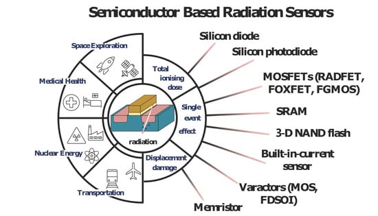
3. Scope of Radiation Measurement

The effects of ionising radiation on electronic circuits as well as on the living human body is very critical and multi-fold. It has been a major concern for various critical applications such as healthcare, mining, avionics, nuclear, high-energy physics, and space applications. Continuous exposure to radiation affects the performance of electronics systems by producing erroneous results and leading to functional failure. It requires accurate estimation of the radiation dose related information (dose rate, accumulated dose) to assess the system performance (known as radiation dosimetry) and subsequently look for corrective measures.
Nowadays many healthcare professionals and assistants are subjected to radiation exposure (X-ray) throughout their careers due to various diagnostic and therapeutic purposes. A regular monitoring of the radiation doses which have been absorbed in the body is required to ensure safety and prevent health hazards. Such exposures concern not only medical personnel but also patients. Most of the radio-therapeutic procedures in oncology recommend precise monitoring of the radiation doses (X-ray, β and proton radiation) administered to the patients. Eventually, it requires in-vivo dosimetry to ascertain a reliable control over the delivered dose, leading to effective treatments. Apart from these, the nuclear facilities and mining industries often require working professionals to work in harsh radiation environments in the presence of radioactive materials. Even though the level of radiation experienced is low, the accumulated amount over the work period could possibly cross the human body’s yearly safe limits and subsequently affect the individual’s health. The occupational dosimetry is absolutely necessary to analyse the total dose of radiation accumulated over time and ensure its adherence to the safety standards.
In addition, the total accumulated dose as well as the real-time dose-rate monitoring are very crucial in the case of interplanetary space flights as well as satellites with scientific payloads orbiting outside the protection provided by the Earth’s atmosphere. During the missions towards low Earth orbit (LEO), geosynchronous equatorial orbit (GEO), and the International Space Station (ISS) near Van Allen radiation belt, various sources of space radiation (predominantly high-energy protons, electrons, and heavy ions) appear as a potential threat to the reliable operation of the complex flight instrumentation. Conventionally, shielding and packaging with appropriate materials are provided to enhance endurance against radiation induced damage. However, the impact of ionising charged particles ( β , p + radiation) aggravate the damage due to nuclear reactions induced within the on-board materials. In addition, the crew members of the space shuttles were regularly subjected to radiation doses throughout the voyages and an especially increased amount during the extravehicular activities. The real-time monitoring of radiation dose helps in establishing the safety of the crew members and functional safety of the on-board electronics for the duration of the mission. Likewise, the dosimeters are also required in ground test facilities to be able to accurately record the absorbed dose during characterisation and subsequently help to model, identify, and forecast the radiation induced effects in devices.
Additionally, high-energy physics experiments involve particle accelerators to generate numerous high-energy particles and photons. Inside the accelerator, the instrumentation requires radiation dosimeters which are capable of measuring very high levels of radiation across the large and distributed facilities. There, the radiation monitors are custom-made and permanently installed across the facilities to enable observation of the radiation dose across the space over a certain period of time. Compared to these, integrated dosimeters help in investigating the unexplored areas facilitating easy access to data with an added benefit of portability. In particular, these avoid inaccuracies due to large cable installations and thus help in characterising and mapping complex radiation fields with higher accuracy in mixed field radiation test facilities such as the CHARM irradiation facility at CERN.
Traditionally, working professionals in healthcare sector and radiation test facilities used to wear passive dosimeter devices that absorb the incident radiation dose over time. Typically, every two to three months, the devices are accessed to determine the accumulated dose related data and possibly causing a delay between the detection and the exposure to radiation. Recently, an increased amount of focus has been given to integrated solutions to facilitate continuous monitoring. In addition, these integrated alternatives provide faster readout electronics and thus ensure rapid and useful counteractive measures.
As mentioned previously, radiation dosimetry is primarily used to measure the absorbed dose of radiation received by the electronic devices. Particularly in the case of space explorations, it provides an estimated overview of dose during the course of a mission. Whatever the context, the dosimetry readings could only provide accumulated dose and sometimes dose-rate related information. Even though the radiation can be monitored in real time, it is not useful for detecting radiation energy and consequently identifying the radiation source types. Considering this inability of the dosimeters, particle detectors are used alongside them for various applications (avionics, automotive and ground stations) to help in characterising the nature of a radiation source and estimating the flux and energy levels of striking particles. During space missions, the flight equipment requires electronics to be optimised in terms of power as well as highly robust and fault tolerant. In the event of certain radiation outburst (solar winds and flares), the particle detectors could possibly identify the threat from the increasing ionising particle flux and subsequently create an alert. In such critical conditions, a multi-core system can be dynamically reconfigured to activate fault tolerant mechanism, ensuring optimal performance with a minimal power budget or even some critical systems can be temporarily switched off.
Furthermore, the particle detectors play a pivotal role in ensuring the reliability of long-distance communications during space missions by detecting SEUs and single-event transients (SETs). The intense charged particles and X-rays originating from solar flares have the potential to interact with electronic equipment, leading to disturbances, interrupts, and subsequent functional failure.
In recent times, several reports have suggested the occurrence of soft errors in flight operations [36], data centres [37,38] and electronic systems [39]. A recent experiment on the feasibility of underwater data [40] has revealed improved reliability and reduced soft-error related failure rate. In such applications where safety is of primary concern, the particle detectors are very crucial in ensuring operational stability and reliability of the on-board electronics.

4. Radiation Measurement Techniques

The radiation events studied here are considered to be randomly distributed over irradiation time following Poisson statistics. Depending on the interaction of semiconductor materials with radiation, the sensors in active mode may respond to an individual quantum of radiation (particle detection) or collective interaction with multiple quanta of radiation over a period of time (dose measurement). However, in passive mode of operation, when there is no external energy source connected to the semiconductor devices and associated circuits, the energy deposited on the devices by individual particle strikes is accumulated over time. Later, when the circuits are biased and the sensors are measured, the accumulated energy gives an estimate of the radiation dose only. As a result, it fails to identify and measure the energy deposited by individual radiation events. In active mode of operation, the radiation sensors and associated circuits are biased using an external energy source and support individual particle detection as well as dose measurement. In active mode, the sensors can operate either in pulse counting method or integral method. In the case of Si-diode or Si-photodiode based detectors, the radiation induced burst of currents are monitored by the readout electronics. The charge collected which is the time integral of the current over the duration of the detection (integral method) provide a measure for the energy deposited. The energy information is used in radiation spectroscopy to estimate the energy spectra. Over a period of time, the integrated charge related data are used to give an indirect measurement of the accumulated dose. In pulse counting mode, the charge collected is compared to a predefined threshold and causes an event to the counter for adding up to the particle detection. In the case of memory based sensors such as static random access memory (SRAM), the critical charge required for a bit-flip in memory elements acts as threshold for particle detection. The readout method used in 3-D NAND based flash memories presents multiple options for threshold comparison and therefore also allows an estimation of energy spectra together with particle detection. In the case of individual MOSFET based sensors, the real-time collection of charge generated from radiation is not convenient, and therefore they have very limited use as particle detectors. These sensor elements themselves act as integrating devices and employ indirect techniques to estimate the total dose information.
The sensors, when operating in integral mode, are usually referred to as radiation dosimeters which helps in the evaluation (directly or indirectly) or measurement of the cumulative radiation quantities (TID, kerma, dose rate and exposure time) [41]. The integration of information can be carried out by the readout electronics (Si-diodes) or by the sensing device themselves (MOSFET based sensors). The readout method follows different techniques such as threshold voltage V T H measurement, current or voltage reference sensing and time-domain (frequency) output and can be categorised based on the sensing device used such as silicon diodes, solid-state photomultipliers (SSPMs), fully depleted silicon-on-insulator (FDSOI) varactors and MOSFET devices such as radiation-sensitive field-effect transistors (RADFETs), field-oxide fieldeffect transistors (FOXFETs), floating-gate MOSFET (FGMOS). Radiation sensors are usually referred to as particle detectors when they are operated in pulse counting mode which helps in identifying radiation events, particularly soft errors in integrated circuits. The methods used are predominantly current or voltage sensing or memory read operations in digital memory structures.
A more detailed individual overview of the various semiconductor based radiation sensors are given below:

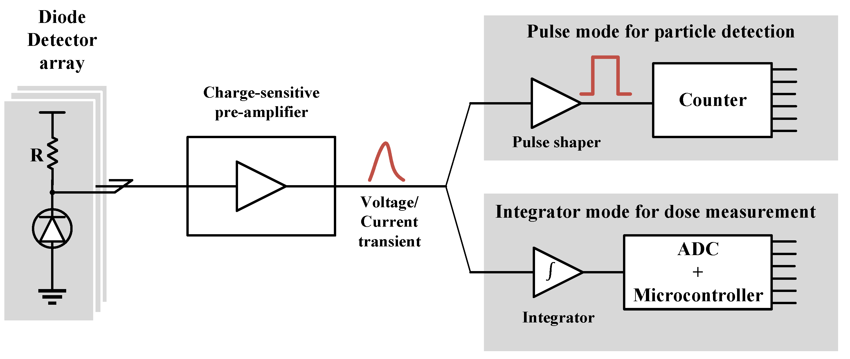
4.1. Silicon Diode Based Radiation Sensors

In this method, the reverse biased p-n junction of a diode is used for dosimetry measurement. The excess charges (minority carriers), which are created due to the interaction with ionising radiation near the depleted region, are swept away through drift in the presence of the electric field over the junction. As illustrated in Figure 3, the excess charges are collected with an external electric field and amplified using a charge-sensitive pre-amplifier. The resulting current or voltage transient from the amplified charge is compared with a threshold and shaped into a pulse to cause a trigger to the digital counter. Thus, while operating in pulse counting mode, the Si-diode based radiation sensors are used as particle detectors. Alternatively, in integral mode of operation a readout circuit measures the transient of voltage or current. The time-integral of the measured quantity provides an estimate of the energy deposited during radiation strike. Thereby, in dosimetry application this energy information provides an indirect measurement of the total accumulated dose on the sensing devices.
Here, the diodes are configured in reverse bias mode of operation which in turn results in a wide depletion layer with reduced leakage current and thus permits higher efficiency in radiation sensing with a linear relationship between the deposited charge and the integrated dose. Si-diode based dosimeters such as single-sided silicon strip detectors [42] and active pixel detectors [43,44] are moderately sensitive and suitable for high-dose radiation measurement as in pulsed radiation fields (X-rays, electron linear accelerators) [41].
Over time, the sensitivity of the diodes reduces due to the damage caused by radiation and need to be re-calibrated to perform effective reliable measurements. During counting of radiation strikes, the readout time needs to be adjusted so that it is able to distinguish between concurrent events. In addition to particle detection and dose measurement, the intensity of the current transient provides an estimate about the energy spectra and linear energy transfer (LET) of the striking high energy particle. More often, an array of detectors is used, which is beneficial in terms of accuracy and to characterise the radiation beam.

4.2. Silicon Photodiodes Based Radiation Sensors

This type of radiation sensor uses Si-photodiodes as the sensing elements. Four types of photodiodes can be used for radiation measurement [45]: the p-n junction photodiode [46], the PIN (p-type, intrinsic, n-type) photodiode [47], the avalanche photodiode [48] and the Schottky photodiode [49]. Compared to standard p-n junction photodiodes, PIN photodiodes provide better sensitivity as the wide intrinsic region helps in achieving high charge generation per radiation strike. The highest sensitivity to radiation among photodiodes is usually obtained in Avalanche photodiodes due to the Avalanche breakdown action. However, the Avalanche photodiode based detectors need larger bias voltage and produce higher levels of noise. Schottky photodiode based radiation detectors are based on compound semiconductor structures (SiC) and provide a fast response time due to low operational capacitance.
The photodiodes can be integrated with SSPMs and are used as an alternate choice for vacuum-based photomultiplier tubes (PMTs) for space, nuclear energy plant and high-energy physics applications [50]. SSPMs are fabricated using an array of Geiger-mode photodiodes on custom CMOS technology. A radiation sensitive scintillator material is coupled to the fabricated SSPM device. An illustration of the CMOS SSPM chip coupled with scintillation material is provided in Figure 4. When an energised radiation particle impinges on the dosimeter surface, the scintillator absorbs the energy and re-emits it in the form of light. The generated photons hit the pixels in the SSPM matrix. A low LET ionising radiation strike activates a few pixels in the matrix, while in the case of a high LET radiation strike a large number of pixels are activated. In response to these, the scintillator coupled SSPM device produces an equivalent amount of current transient which is detected by the readout interface. Thereafter, the transients are recorded to count the radiation events. Similar to Si-diode based radiation sensors, the time integral of the current could also be digitised using an analogue-to-digital converter (ADC) to perform an indirect estimation of accumulated dose.
The number of photodiodes activated is proportional to the energy deposited due to the strike of high-energy radiation. Compared to PMTs, the SSPM based dosimeters are compact, lightweight and can be integrated with on-chip CMOS readout circuits [50,51]. The digitised output provides an estimation of the absorbed dose and deposited energy spectra and LET of the radiation particle.

4.3. Radiation Sensitive MOSFET Devices

The electrical characteristics of the MOSFET devices, particularly the mobility and the threshold voltage ( V T H ), experience changes due to the radiation strike from high-energy particles. The radiation induced field-oxide trapped charges produce a negative change in V T H for both pMOS and nMOS, whereas, in case of interface trap charges, pMOS see a negative change but nMOS sees a positive change in V T H [52]. Initially, the MOSFET based dosimeters were used in space [8] where the pMOS transistors were used in diode configuration to track and measure radiation dose by means of observing the V T H shift. A readout circuit was provided to track the voltage difference between the gate and source terminal ( V G S ) of the diode-mode pMOS transistors and to measure the change in threshold voltage. As predicted in [53], the absolute value of the threshold voltage shift is proportional to the gate-oxide thickness squared ( t O X 2 ). In order to increase the radiation sensitivity and ensure a better response, the RADFETs were provided with very thick gate oxide, which were used in nuclear facilities [54,55]. The devices were also used for radiation dosimetry in medical diagnosis and radiotherapy treatments [56,57]. The fabrication of RADFET devices require an ad hoc process, which makes it difficult to implement them with commercial CMOS technologies evolving to thinner oxides. The radiation sensitivity is also limited by the packaging materials. Additionally, the changing temperature effects of the MOSFET parameters (carrier mobility, V T H , etc.) make it difficult to isolate and identify radiation induced variations which in turn affects the accuracy of the dosimeter readings [58].
To overcome the lower sensitivity of the RADFET devices, FOXFETs are developed where the field oxide (used as the passivation layer to isolate CMOS circuits) is utilised instead of the gate oxides [59]. The thickness of the field oxide is usually in the range of 400–600 nm [59], and therefore it facilitates an increased amount of trapped charge generation when exposed to radiation. A view of the cross-section of the FOXFET device is provided in Figure 5a. Compared to RADFET devices, the higher number of trapped charges in FOXFET gate-oxide cause a much larger change in V T H . As shown in Figure 5b, the V T H of the FOXFET device is measured by forcing a constant current through the device and the V T H shift gives an estimate of the accumulated dose. The use of field oxide also made it easy to implement the device in any CMOS technology and integrate them together with the readout circuits. However, similar to RADFETs [60], the temperature dependency of the electrical parameters is still problematic with FOXFETs leading to erroneous dose readings. To mitigate the issues related to temperature variations, differential architectures are used where bias currents were designed with reduced temperature coefficients [61,62]. RADFET and FOXFET devices require very thick gate-oxide as well as large area to increase radiation sensitivity. These are therefore used as discrete devices or needed to be implemented in custom CMOS process.
Alternatively, FGMOS devices have also being explored for various dosimetry applications [15,63,64,65]. The floating gate (FG) structures can be implemented by connecting the poly-silicon gate of a MOS-capacitor to the gate of sensing MOSFET device in standard CMOS technology [66] as shown in in Figure 6a. Otherwise, it can also be implemented by using an additional insulated poly-silicon gate in a custom two poly CMOS process [67] as shown in Figure 6b. Thereby, in this process a capacitance is also formed alongside the gate of the FGMOS device. The capacitance is used to pre-charge the FG prior to irradiation by injection of carriers by avalanche process or by tunneling through the gate-oxide [64]. When exposed to ionising radiation, charges are generated which accumulate in the oxide region and neutralise the initial charge on the FG. This results in a change in V T H [63] and the readout circuit integrated on-chip with the sensing devices measures the V T H shift and provides a proportional voltage [65,68] or current output [69]. In order to compensate for temperature dependence of the V T H shift, a typical MOSFET with similar dimensions is used as a reference to monitor the temperature induced parameter variation. The sensing FGMOS and the typical MOSFET are used in a differential configuration and therefore it cancels out temperature induced changes happening in both devices as reported in [15,65]. Alternatively, the FGMOS devices are used to implement current starved inverters and provide a frequency output, the change of which is proportional to the total accumulated dose [66,67]. FGMOS based dosimeters are typically very sensitive to radiation dose and therefore the sensor responses are saturated and suffer from non-linearity for dose levels more than 100 Gy. These provide high resolution ( 500 mrad [67]), but the application of these sensors is only limited to low dose level (10–100 Gy) measurement. Compared to RADFET and FOXFET devices, FGMOS based radiation sensors are preferred in recent times considering the ease of on-chip integration with the peripheral circuits. FGMOS dosimeters are also being investigated for high-dose level monitoring in accelerator environments using the repeated measurement technique as reported in [70,71].

4.4. SRAM Based Radiation Monitor

In the presence of radiation hazards, SEUs can easily affect the circuits that store data, for example, flip-flop, RAM, and storage circuits. Among these, SRAM (Static Random-Access Memory) is the most typical circuit to monitor SEUs in electronic systems. It is composed by two cross coupled inverters which create a stable bi-states structure, as shown in Figure 7. If one side of the circuit is hit by a particle, the collected charge from the particle will trigger the positive feedback of the inverters and lead to a bit flip (i.e., upset).
Moreover, SRAM is the most common device for SEU fault monitoring in processing systems. It has unique advantages such as a simple and controllable interface, low cost, high density (cells per unit area), low power consumption, and can be embedded on the same technology or chip as the device being monitored, like a microprocessor. The principle of SRAM based particle detectors is simply searching the memory for bit flips. These can be single-cell upsets (SCUs) or multi-cell upsets (MCUs). As technologies have scaled down, single particle strikes can upset multiple cells simultaneously, depending on the particle energy. As indicated in [72], the ratio of MCU and SCU can be used to estimate the particle energy.
The radiation detectors used in ESA [73], CERN [74] and satellite mission [75] have embedded multiple commercial off-the-shelf (COTS) SRAMs for SEU monitoring. The first purpose of these circuits is to monitor the radiation environment in space and ground facilities to guarantee that the environment radiation intensity is in line with the design specification of the system and the data are reliable. The second purpose is to monitor the flux, beam profile and beam homogeneity at particle accelerator facilities such as RADEF and CHARM [73]. Thirdly, for cross facility SEE testing, adding an SRAM to the system enables the cross-calibration of the variation at different facilities, which increases the data fidelity [76]. Fourthly, applying radiation hardened devices improves the robustness to SEE. However, complex systems still inevitably contain COTS components to balance cost and performance. Therefore, an SEU monitor is needed for the system to guarantee the error rate of the system stays below the manageable limit.
To achieve a higher SEU sensitivity and resolution, SRAMs fabricated in smaller technology nodes (65 nm and less) can be used. In recent work [77,78], a broad variety of COTS SRAM chips and FPGAs were tested. The results showed that 16 to 65 nm SRAM have high SEU cross sections. Alternatively, decreasing the supply voltage can increase the SEU sensitivity [79], and every type of particle shows a different sensitive range when varying the voltage supply [80]. This enables sufficient calibration for the radiation monitor to analyse the intensity and type of radiation source by sweeping the supply voltage [79,80]. However, commercial chips have an embedded voltage regulator between the voltage supply and the core circuit. This regulator can handle a certain range of input voltages to a constant level. It becomes nonlinear and unpredictable outside of its voltage range, especially for more advanced technologies. Henceforth, this approach is less feasible with commercial memories and calls for custom designed SRAM sensors.
Finally, most COTS SRAMs have an embedded error-correcting code feature, which can correct some SEUs complicating or obstructing its use as a radiation monitor [81]. Additionally, when testing for MCUs, one needs to be aware that the physical order of the cell array may differ from the logical (address) order through scrambling. The susceptibility of COTS SRAM circuits to SEL induced failures are more in comparison to custom designed SRAM sensors. The COTS SRAM circuits are typically aimed to achieve a high density. Therefore, the wells and doping areas are closer than normal chips, making them more prone to latchup induced circuit failures.

4.5. Built-In Current Sensor Based Radiation Detectors

In this method, the radiation induced transient current pulses are detected by means of monitoring the supply voltage [82,83,84] or measuring the supply current externally using current monitors [85,86]. The methods are not reliable and effective to identify the location of the transient induced logic state errors in an array of memory cells. The issue has been resolved by introducing built-in current sensor (BICS) circuits [87,88] adjacent to each row and column of the memory cell array to locate the transient induced faults. However, the proposed techniques involved distributed synchronous BICS circuits and subsequently failed to detect short and intermittent current transients in the supply. This method, as illustrated in Figure 8a, uses high-speed asynchronous BICS circuits which are placed inline with the power supply of the devices and therefore it affects the systems performance by injecting noise and disturbances into the power supply.
As a remedy, a bulk connected BICS as shown in Figure 8b, is proposed in [89] with an increased sensitivity towards particle strike, but reduced interference with the system’s performance. The bulk connected BICS circuits consist of a pMOS activated BICS (pBICS) and an nMOS activated BICS (nBICS). At the onset of a radiation strike, the excess charges travel through the reversed biased bulk junction and activate the respective current sensors. Recently, similar approaches have been explored in [90,91,92,93,94,95] and a further improvement has been proposed in [96] by using triple-well CMOS technologies.
The primary advantage of utilising bulk connected BICS circuits is that they are able to locate transient induced faults and thus can effectively activate the mitigation mechanisms in the respective memory cells. However, it is ineffective in characterising the particle flux and suffers from the inability of directly providing any information about the deposited energy. Moreover, the current sensors are susceptible to substrate noise and subsequently may induce erroneous results.

4.6. 3-D NAND Flash Based Radiation Monitors

FGMOS devices have been exploited to realise various non-volatile memory architectures [97,98] and have been successfully explored for data storage applications in space [99,100,101]. In addition, the FG based devices are very effective in dosimetry applications to measure the amount of TID in a radiation environment [14,70,102]. Recently, the FG based flash memories appeared as a viable alternative [103,104,105] to be utilised as particle detectors.
As the ionising particle impinges on the devices in flash memories, the excess charge impacts the FG based storage element and subsequently cause threshold voltage shift in the FGMOS devices inside the memory cell. Nowadays, the readout circuits provided inside the flash memory cells can identify the radiation event from the change in threshold voltage and collectively measures the number of upsets similar to SRAM based radiation monitors. In the case of flash memory based architectures, each memory unit is configured with multi-bit (4-bit or 8-bit binary code) storage cells which are capable of measurement based characterisation of multi-level threshold voltage distributions. As a result, these types of particle detectors provide an estimate of charge deposited due to the interaction with radiation by accurately measuring the threshold voltage shifts [106]. Unlike the SRAM based solutions, it is feasible to characterise the LET of the striking particle in flash memories and extract information about the nature of radiation (heavy ion, proton [107], neutron [108]).
Due to the non-volatile nature of memory cells, the NAND flash-based particle detectors facilitate low power dissipation and offline passive mode of operation. Compared to 2-D structures, dense 3-D integration of flash memory cells is beneficial ensuring higher detection efficiency [109]. As illustrated in Figure 9, the affected memory elements provide the information about the angle of incidence and the track of radiation strike as well [110]. The further study of the pattern of the threshold voltage shifts of the devices arranged in a 3-D volume along the track of radiation strike provides more details about the uniformity of the ionising radiation beam [109,110].
Although the 3-D NAND flash-based particle detectors are beneficial in terms of efficiency and added features, the complexity of integration with planar CMOS technologies presents a difficulty in implementation. In addition, the device noise affects the accuracy of estimation of energy absorbed in radiation requiring complex readout schemes targeting low noise mixed-signal readout implementations [111]. Another notable drawback is the long readout time needed to process a very large number of memory cells which also leads to an increased expenditure of power.

4.7. Memristor Based Radiation Sensor

Memristor based resistive random-access-memory (ReRAM) technology has been brought into focus during the last decade [112,113] considering its non-volatile property and ability to perform in-memory computing both in digital and analog domain operations. Typically, a ReRAM cell consists of a memristor element, a two terminal non-linear resistive device prepared by sandwiching a resistive material (TiO 2 , ZrO 2 , NiO, etc.) between two metal electrodes. The value of its resistance (known as memresistance) is not constant and changes depending on the magnitude, polarity and duration time of the applied voltage across its terminals, or the current passed through it. It shows a hysteretic behaviour in its voltage-current characteristics and the memresistance value of the devices are non-volatile in nature.
Under ionising radiation, the electrical properties of the elements are subjected to change due to the processes through ionic and molecular dissociations and defect formations, unlike charge formation that happens in CMOS devices. The initial investigations [114,115,116] have showed very little dependence of memristor devices on radiation effects due to its ultra-thin film structures. However, “ μ m-thick” TiO 2 based elements showcased increased radiation detection ability [117].
As illustrated in [117], each memristor is connected to a switched capacitor element to charge the capacitors. As shown in Figure 10, each memristor is switched on in monitoring mode using the voltage V i n . When exposed to radiation, the memresistance value changes and it modifies the charging time-constant when the capacitor is charged through the memristor in detection mode. The effects of radiation can be observed after the detection time window, when the capacitor charges to a voltage level different from what is expected in absence of radiation. After the detection mode, each memristor is switched off using voltage V r e s e t and the capacitor is discharged. An array of such units are placed inside a crossbar based structure and the readout circuit registers the change in resistivity in each row of sensors. Although these sensor circuits are highly dense and consume very little power compared to CMOS based detectors, the primary bottleneck is a relatively slower response time causing hindrance to real-time sensing. Moreover, these devices are dose rate integrating devices and therefore can hardly resolve individual radiation strikes or identify different incident energies.

4.8. Variable Capacitor Based Radiation Sensor

Variable capacitors or varactors implemented in CMOS technologies (bulk-CMOS and silicon-on-insulator) are viable alternatives to diode and MOSFET based solutions used for radiation sensing. Similar to these solid-state dosimeters, the capacitor based sensors measure the accumulated dose depending on the ionising effects happening inside the dielectric material. Although MOSFET based dosimeters are very popular in terms of reliability and added features, its DC operation methods are very sensitive to various disturbances—in particular to thermal and flicker noise sources [32]. In comparison, variable capacitor based dosimeters have the capability to overcome the noise limits and accomplish ultra-high sensitivity as they employ AC measurement techniques [118,119]. When exposed to radiation, such a sensor exhibits a change in capacitance-voltage (C-V) characteristics due to trapped charges near the Si/SiO 2 interface. Subsequently, it results in a different capacitance value in depletion mode, for a given voltage applied between its terminals. Several studies [120,121,122,123] have been carried out on MOS-cap based structures implemented in bulk-CMOS technologies to research the feasibility of radiation dose measurement.
For a given dose of radiation, the sensitivity of the capacitor based detectors relies on the thickness of the dielectric layer and the trapped charge density near the interface. However, the scaling trend of CMOS technologies makes it difficult for MOS-based capacitors to achieve better sensitivity as the oxide thickness is traded off with capacitance tuning [123]. In recent times, the development of FDSOI technology has enabled the varactors to achieve high sensitivity as well as high capacitance per unit area. In the presence of ionising radiation, the thick buried-oxide (BOX) layer beneath the varactor elements collects the radiation induced charges [118]. The resulting shift in capacitance value is measured using a readout circuit. As illustrated in Figure 11, an LC resonator equipped with the radiation sensing capacitor provides a frequency output and the change of which is proportional to the accumulated dose [119]. FDSOI based radiation sensitive varactors are very effective in low dose measurements with very high sensitivity [124]. The radiation sensors are also investigated as reported in [125] for in vivo dosimetry in radiation cancer therapy.

5. Sensor Performance

Radiation sensors, namely both dosimeters and particle detectors, are very effective tools to measure, evaluate or characterise various radiation parameters (energy spectra, fluence, LET, etc.) and the resulting effects (absorbed dose, bit-upsets, etc.). The use of semiconductor technologies has enabled sensor systems with the flexibility to be integrated with microelectronics and achieve better sensitivity with improved signal processing techniques. Semiconductor based sensors are intrinsically reusable but suffer from a gradual loss of sensitivity caused by radiation induced damages (crystal defects, leakage current, etc.) during their operation time. For a given radiation environment, the increasing leakage current can be compensated by using cooling, and the performance degradation may be restored by thermal annealing, thereby extending the sensor’s lifespan. In case of dosimetry, the semiconductor based sensors are in general used for relative measurement and need calibration with respect to absolute standards to ensure accuracy of the readings.
A comparative study of the semiconductor based radiation sensors based on their different features, methods and technologies is provided in Table 1. Radiation sensitive MOSFETs such as RADFETs and FOXFETs primarily employ DC measurement techniques, namely V T H measurement and need simple readout architectures. However, the static power consumption adds to the power overhead. The front-end electronics are more complex in the case of diode based detectors operating in pulse mode or integration mode. FGMOS structures which require charge injectors and the varactors using AC methods employ a similar level of complexity. As mentioned in Table 1, the most complex signal processing techniques and readout algorithms are employed in 3-D NAND flash and ReRAM memory based radiation sensors. Consequently, it results in increased power overhead, but not in the case of memristor based ReRAM as the memory array can be configured in passive mode with very low power consumption. Among the semiconductor based sensors, the FGMOS devices, ReRAM and FDSOI varactors, exhibit the highest sensitivity towards radiation dose. Nevertheless, the measures and parameters exhibit non-linearity with respect to the accumulated dose, and the effective range of dose for which they could be used is significantly lower. These sensors are primarily intended to be used in very low dose applications such as occupational dosimetry or therapeutic procedures. However, the FGMOS based devices as demonstrated in [70], support repeated measurements in auto-recharge mode and can be configured to record higher dose levels in accelerator environments. Although in such cases, longer readout times can possibly accumulate low frequency flicker noise components and degrade the signal-to-noise ratio (SNR) performance and reduce the radiation dosimeter’s resolution.
A summary of different sensing principles and field of applications of the different semiconductor based radiation sensors is provided in Table 2. In case of applications involving high rates of radiation events, the sensors require a fast readout time. Therefore, multiple sensor elements are used in parallel with segmentation, but eventually increase the power consumption. Sensors implemented in planar arrays such as silicon strip detectors (Si-diodes or Si-photodiodes) and SRAM based monitors and 3-D array structures namely the NAND flash memories effectively also help in characterising the incident particle’s energy spectra. In addition, these sensor arrays could estimate the LET of charged particles and incidence angle of a radiation strike by employing subsequent signal processing on the sensor readings.

6. Discussion

This review article summarises the semiconductor based radiation sensors (dosimeter and particle detectors) developed in the last few decades for radiation (TID and SEEs) measurement. Ionising radiation is a severe concern for reliable operation of electronic systems, particularly in data centres, flight control systems, satellite payloads and scientific instruments used in various applications. Under the impact of radiation, the performance of the electronic systems degrades over the period of operation and eventually the system fails in extreme conditions. The radiation dosimeters essentially help in qualifying the radiation hardness of the electronic systems, as well as monitoring and characterising the radiation field for accurate modelling and implementing mitigation steps. Particle detectors primarily identify radiation induced logic errors, memory upsets and interrupts in electronic systems, and subsequently help in error correction in order to ensure reliability and resilience against harsh radiation. In addition, applications involving occupational and medical therapy related radiation hazards require the dosimeters to ensure that the absorbed dose for the working professionals and patients is maintained within the recommended limits.
In this article, different methods of radiation dosimetry as well as particle detection are explored, and the modes of operations are discussed with merits and demerits. So far, various semiconductor devices and design techniques for integrated sensors are adopted and experimented with to find out the effectiveness, reliability, and robustness of radiation detection. Compared to various techniques of low dose-level dosimetry, the FGMOS based sensors are increasingly being explored and improved considering integrated applications such as in vivo radiation therapy and occupational radiation dosimetry [15,63,64,65], whereas silicon diodes and photomultipliers are still the preferred choice for high-dose level measurement. In case of particle detectors, the SRAM based radiation monitors are preferred over the rest considering ease of CMOS integration and memory storage [126,127]. However, in the future, once the methods are developed for on-chip 3-D integration, the 3-D flash memories could present a viable option. In addition, recent times have seen the emergence of new semiconductor devices and memory technologies as a result of continuous scientific efforts [128,129]. Recently, silicon photonic devices have also been experimented to find out the radiation effects [130,131,132,133]. The radiation sensors based on Si-diode, Si-photodiode, MOSFET devices with planar structures (RADFET, FOXFET, FGMOS) and SRAM are already well investigated, but still their performances can possibly be improved in the future with better readout electronics. A few (3-D NAND flash, memristor and FDSOI varactor) could possibly help in realising new improved methods for radiation sensing. However, this would need further investigation, radiation tests and qualifications to explore the potential and possible limitations of these devices.

Author Contributions

A.K., J.W., J.P., V.D.S. and P.L. formulated this review. A.K. and J.W. performed the literature analysis and prepared the manuscript with input from all authors. All authors have read and agreed to the published version of the manuscript.

Funding

This work is funded by the European Union Horizon 2020 Research and Innovation Programme under grant agreement number 721624 “RADSAGA”.

Institutional Review Board Statement

Not applicable.

Informed Consent Statement

Not applicable.

Data Availability Statement

Not applicable.

Conflicts of Interest

The authors declare no conflict of interest.

Abbreviations

The following abbreviations are used in this manuscript:
MOSFETmetal-oxide-semiconductor fieldeffect transistors
CMOSComplementary MOSFET
pMOSp-channel MOSFET
nMOSn-channel MOSFET
TIDTotal ionising dose
SEESingle-event effect
DDDisplacement damage
NIELNon-ionising energy loss
SEUSingle-event upset
SETSingle-event transient
SEFISingle-event functional interrupt
SELSingle-event latchup
SEGRSingle-event gate rupture
SEBSingle-event burnout
SRAMStatic random access memory
RADFETRadiation-sensitive fieldeffect transistor
FOXFETField-oxide fieldeffect transistor
FGMOSFloating-gate MOSFET
SSPMSolid-state photomultiplier
FDSOIFully-depleted silicon-on-insulator
LETLinear energy transfer
FGFloating gate
PMTPhotomultiplier tube
ADCAnalog-to-digital converter
SCUSingle-cell upset
MCUMulti-cell upset
COTS  Commercial off-the-shelf
BICS  Built-in current sensor
pBICS  pMOS activated BICS
nBICS  nMOS activated BICS
ReRAM  Resistive random-access-memory
BOX  Buried-oxide
LEO   Low Earth orbit
GEO  Geosynchronous equatorial orbit
ISS  International Space Station
SNR  Signal-to-noise ratio

References

  1. Rossin, A.D. Dosimetry for Radiation Damage Studies. IEEE Trans. Nucl. Sci. 1964, 11, 130–136. [Google Scholar] [CrossRef] [Green Version]
  2. Kloepper, R.M. Neutron and Gamma-Ray Rate Sensitivities of Several Dynamic Detectors Used in Radiation Effects. IEEE Trans. Nucl. Sci. 1964, 11, 137–144. [Google Scholar] [CrossRef]
  3. Beezhold, W.; Beutler, D.; Garth, J.; Griffin, P. A review of the 40-year history of the NSREC’S dosimetry and facilities session (1963–2003). IEEE Trans. Nucl. Sci. 2003, 50, 635–652. [Google Scholar] [CrossRef]
  4. Hester, D.L.; Glower, D.D.; Overton, L.J. Use of Ferroelectrics for Gamma-Ray Dosimetry. IEEE Trans. Nucl. Sci. 1964, 11, 145–154. [Google Scholar] [CrossRef]
  5. Birdsall, R.L.; Binder, D.; Peffley, W.M. A Strain Gage Dosimeter for Pulsed Radiation Environment. IEEE Trans. Nucl. Sci. 1968, 15, 346–349. [Google Scholar] [CrossRef]
  6. Sukis, D.R. Thermoluminescent Properties of CaF2: Dy TLD’S. IEEE Trans. Nucl. Sci. 1971, 18, 185–189. [Google Scholar] [CrossRef]
  7. Wrobel, T.F.; Berger, R.A. Silicon Calorimeter System for Gamma and Electron-Beam Radiation Dosimetry. IEEE Trans. Nucl. Sci. 1975, 22, 2314–2318. [Google Scholar] [CrossRef]
  8. Adams, L.; Holmes-Siedle, A. The Development of an MOS Dosimetry Unit for Use in Space. IEEE Trans. Nucl. Sci. 1978, 25, 1607–1612. [Google Scholar] [CrossRef]
  9. Zoutendyk, J.A.; Malone, C.J. Field Funneling and Range Straggling in Partially Depleted Silicon Surface-Barrier Detectors. IEEE Trans. Nucl. Sci. 1984, 31, 1101–1105. [Google Scholar] [CrossRef]
  10. Brucker, G.J.; Stassinopoulos, E.G.; Van Gunten, O.; August, L.S.; Jordan, T.M. The Damage Equivalence of Electrons, Protons, and Gamma Rays in MOS Devices. IEEE Trans. Nucl. Sci. 1982, 29, 1966–1969. [Google Scholar] [CrossRef]
  11. Stapor, W.J.; August, L.S.; Wilson, D.H.; Oldham, T.R.; Murray, K.M. Proton and Heavy-Ion Radiation Damage Studies in MOS Transistors. IEEE Trans. Nucl. Sci. 1985, 32, 4399–4404. [Google Scholar] [CrossRef]
  12. Rosenfeld, A.; Carolan, M.; Kaplan, G.; Allen, B.; Khivrich, V. MOSFET dosimeters: The role of encapsulation on dosimetric characteristics in mixed gamma-neutron and megavoltage X-ray fields. IEEE Trans. Nucl. Sci. 1995, 42, 1870–1877. [Google Scholar] [CrossRef]
  13. O’Connell, B.; Conneely, C.; McCarthy, C.; Doyle, J.; Lane, W.; Adams, L. Electrical performance and radiation sensitivity of stacked PMOS dosimeters under bulkbias control. IEEE Trans. Nucl. Sci. 1998, 45, 2689–2694. [Google Scholar] [CrossRef]
  14. Scheick, L.; McNulty, P.; Roth, D. Dosimetry based on the erasure of floating gates in the natural radiation environments in space. IEEE Trans. Nucl. Sci. 1998, 45, 2681–2688. [Google Scholar] [CrossRef]
  15. Martin, M.; Roth, D.; Garrison-Darrin, A.; McNulty, P.; Andreou, A. FGMOS dosimetry: Design and implementation. IEEE Trans. Nucl. Sci. 2001, 48, 2050–2055. [Google Scholar] [CrossRef]
  16. Zoutendyk, J.A.; Malone, C.J.; Smith, L.S. Experimental Determination of Single-Event Upset (SEU) as a Function of Collected Charge in Bipolar Integrated Circuits. IEEE Trans. Nucl. Sci. 1984, 31, 1167–1174. [Google Scholar] [CrossRef]
  17. Farrell, G.E.; McNulty, P.J. Microdosimetric Aspects of Proton-Induced Nuclear Reactions in Thin Layers of Silicon. IEEE Trans. Nucl. Sci. 1982, 29, 2012–2016. [Google Scholar] [CrossRef]
  18. Rosenfeld, A. MOSFET Dosimetry on Modern Radiation Oncology Modalities. Radiat. Prot. Dosim. 2002, 101, 393–398. [Google Scholar] [CrossRef]
  19. Fleetwood, D.M. Radiation Effects in a Post-Moore World. IEEE Trans. Nucl. Sci. 2021, 68, 509–545. [Google Scholar] [CrossRef]
  20. Benedetto, J.M.; Boesch, H.E.; McLean, F.B.; Mize, J.P. Hole Removal in Thin-Gate MOSFETs by Tunneling. IEEE Trans. Nucl. Sci. 1985, 32, 3916–3920. [Google Scholar] [CrossRef]
  21. Saks, N.S.; Ancona, M.G.; Modolo, J.A. Generation of Interface States by Ionizing Radiation in Very Thin MOS Oxides. IEEE Trans. Nucl. Sci. 1986, 33, 1185–1190. [Google Scholar] [CrossRef] [Green Version]
  22. Dodd, P.E.; Shaneyfelt, M.R.; Schwank, J.R.; Felix, J.A. Current and Future Challenges in Radiation Effects on CMOS Electronics. IEEE Trans. Nucl. Sci. 2010, 57, 1747–1763. [Google Scholar] [CrossRef]
  23. Dodd, P.; Shaneyfelt, M.; Felix, J.; Schwank, J. Production and propagation of single-event transients in high-speed digital logic ICs. IEEE Trans. Nucl. Sci. 2004, 51, 3278–3284. [Google Scholar] [CrossRef]
  24. Stassinopoulos, E.; Raymond, J. The space radiation environment for electronics. Proc. IEEE 1988, 76, 1423–1442. [Google Scholar] [CrossRef]
  25. Barth, J.; Dyer, C.; Stassinopoulos, E. Space, atmospheric, and terrestrial radiation environments. IEEE Trans. Nucl. Sci. 2003, 50, 466–482. [Google Scholar] [CrossRef] [Green Version]
  26. Normand, E. Single-event effects in avionics. IEEE Trans. Nucl. Sci. 1996, 43, 461–474. [Google Scholar] [CrossRef]
  27. Dunn, T.S.; Williams, J.L. Comparison of Cobalt-60 and Electron Accelerators for Radiation Sterilization. IEEE Trans. Nucl. Sci. 1979, 26, 1776–1783. [Google Scholar] [CrossRef]
  28. Piroue, P.A. Radiation Detectors in High Energy Physics. IEEE Trans. Nucl. Sci. 1966, 13, 54–59. [Google Scholar] [CrossRef]
  29. Bruzzi, M. Radiation damage in silicon detectors for high-energy physics experiments. IEEE Trans. Nucl. Sci. 2001, 48, 960–971. [Google Scholar] [CrossRef]
  30. Oldham, T.; McLean, F. Total ionizing dose effects in MOS oxides and devices. IEEE Trans. Nucl. Sci. 2003, 50, 483–499. [Google Scholar] [CrossRef] [Green Version]
  31. Meisenheimer, T.; Fleetwood, D. Effect of radiation-induced charge on 1/f noise in MOS devices. IEEE Trans. Nucl. Sci. 1990, 37, 1696–1702. [Google Scholar] [CrossRef]
  32. Fleetwood, D.; Meisenheimer, T.; Scofield, J. 1/f noise and radiation effects in MOS devices. IEEE Trans. Electron Devices 1994, 41, 1953–1964. [Google Scholar] [CrossRef]
  33. Baumann, R. Radiation-induced soft errors in advanced semiconductor technologies. IEEE Trans. Device Mater. Reliab. 2005, 5, 305–316. [Google Scholar] [CrossRef]
  34. Moll, M. Displacement Damage in Silicon Detectors for High Energy Physics. IEEE Trans. Nucl. Sci. 2018, 65, 1561–1582. [Google Scholar] [CrossRef]
  35. Rizzolo, S.; Le Roch, A.; Marcelot, O.; Corbière, F.; Paillet, P.; Gaillardin, M.; Magnan, P.; Goiffon, V. High Displacement Damage Dose Effects in Radiation Hardened CMOS Image Sensors. IEEE Trans. Nucl. Sci. 2020, 67, 1256–1262. [Google Scholar] [CrossRef]
  36. Neutron-Induced Single Event Upset (SEU) FAQ. Microsemi Corporation. Available online: https://www.microsemi.com/document-portal/doc_view/130760-neutron-seu-faq (accessed on 22 June 2021).
  37. Cisco 12,000 Single Event Upset Failures Overview and Work Around Summary. Cisco Systems. Available online: https://www.cisco.com/c/en/us/support/docs/field-notices/200/fn25994.html (accessed on 22 June 2021).
  38. Ziegler, J.; Puchner, H. SER–History, Trends and Challenges: A Guide for Designing with Memory ICs; Cypress: San Jose, CA, USA, 2004. [Google Scholar]
  39. Frost, C. When the Chips Are down…Neutron Detection with Micro-Pattern Gaseous Detectors, CERN. Available online: https://indico.cern.ch/event/265187/contributions/590981/attachments/472030/653484/CHIPIR-CERN151013.pdf (accessed on 22 June 2021).
  40. Microsoft Finds Underwater Datacenters are Reliable, Practical and Use Energy Sustainably. Microsoft Corporation. Available online: https://news.microsoft.com/innovation-stories/project-natick-underwater-datacenter (accessed on 22 June 2021).
  41. Ravotti, F. Dosimetry Techniques and Radiation Test Facilities for Total Ionizing Dose Testing. IEEE Trans. Nucl. Sci. 2018, 65, 1440–1464. [Google Scholar] [CrossRef] [Green Version]
  42. Kasahara, S.; Mitani, T.; Ogasawara, K.; Takashima, T.; Hirahara, M.; Asamura, K. Application of single-sided silicon strip detector to energy and charge state measurements of medium energy ions in space. Nucl. Instrum. Methods Phys. Res. Sect. Accel. Spectrometers Detect. Assoc. Equip. 2009, 603, 355–360. [Google Scholar] [CrossRef]
  43. Havranek, M.; Benka, T.; Hejtmanek, M.; Janoska, Z.; Kafka, V.; Kopecek, J.; Kuklova, M.; Marcisovska, M.; Marcisovsky, M.; Neue, G.; et al. MAPS sensor for radiation imaging designed in 180 nm SOI CMOS technology. J. Instrum. 2018, 13, C06004. [Google Scholar] [CrossRef]
  44. Wong, W.; Alozy, J.; Ballabriga, R.; Campbell, M.; Kremastiotis, I.; Llopart, X.; Poikela, T.; Sriskaran, V.; Tlustos, L.; Turecek, D. Introducing Timepix2, a frame-based pixel detector readout ASIC measuring energy deposition and arrival time. Radiat. Meas. 2020, 131, 106230. [Google Scholar] [CrossRef]
  45. Damulira, E.; Yusoff, M.N.S.; Omar, A.F.; Mohd Taib, N.H. A review: Photonic devices used for dosimetry in medical radiation. Sensors 2019, 19, 2226. [Google Scholar] [CrossRef] [Green Version]
  46. Zhang, L.H.; Platt, S.P.; Edwards, R.; Allabush, C. In-situ neutron dosimetry for single-event effect accelerated testing. IEEE Trans. Nucl. Sci. 2009, 56, 2070–2076. [Google Scholar] [CrossRef]
  47. Duan, Y.; Yao, Y.; Li, Z.; Zhou, J.; Huang, P.; Gao, W. SENSROC12: A Four-Channel Binary-Output Front-End Readout ASIC for Si-PIN-Based Personal Dosimeters. IEEE Trans. Nucl. Sci. 2019, 66, 1976–1983. [Google Scholar] [CrossRef]
  48. Becker, H.N.; Farr, W.H.; Zhu, D.Q. Radiation Response of Emerging High Gain, Low Noise Detectors. IEEE Trans. Nucl. Sci. 2007, 54, 1129–1135. [Google Scholar] [CrossRef]
  49. Bertuccio, G.; Puglisi, D.; Macera, D.; Di Liberto, R.; Lamborizio, M.; Mantovani, L. Silicon carbide detectors for in vivo dosimetry. IEEE Trans. Nucl. Sci. 2014, 61, 961–966. [Google Scholar] [CrossRef]
  50. Chen, X.J.; Johnson, E.B.; Staples, C.J.; Chapman, E.; Alberghini, G.; Benton, E.; Christian, J.F. Space Dosimeters Based on CMOS SSPM Technology. IEEE Trans. Nucl. Sci. 2010, 57, 3450–3455. [Google Scholar] [CrossRef]
  51. Chen, X.J.; Johnson, E.B.; Stapels, C.J.; Fernandez, D.; Podolsky, M.; Vogel, S.; Christian, J.F. Effects of Proton Radiation on Noise Performance in Solid-State Photomultipliers. IEEE Trans. Nucl. Sci. 2016, 63, 1109–1116. [Google Scholar] [CrossRef]
  52. Barnaby, H.J. Total-Ionizing-Dose Effects in Modern CMOS Technologies. IEEE Trans. Nucl. Sci. 2006, 53, 3103–3121. [Google Scholar] [CrossRef]
  53. McGarrity, J.M. Considerations for Hardening MOS Devices and Circuits for Low Radiation Doses. IEEE Trans. Nucl. Sci. 1980, 27, 1739–1744. [Google Scholar] [CrossRef] [Green Version]
  54. Holmes-Siedle, A.; Adams, L.; Leffler, J.S.; Lindgren, S.R. The RADFET system for real-time dosimeter in nuclear facility. IEEE Trans. Nucl. Sci. 1983, 26, 025004. [Google Scholar]
  55. RADFET: A review of the use of metaloxide-silicon devices as integrating dosimeters. Int. J. Radiat. Appl. Instrum. Part C Radiat. Phys. Chem. 1986, 28, 235–244. [CrossRef]
  56. Butson, M.J.; Rozenfeld, A.; Mathur, J.N.; Carolan, M.; Wong, T.P.; Metcalfe, P.E. A new radiotherapy surface dose detector: The MOSFET. Med. Phys. 1996, 23, 655–658. [Google Scholar] [CrossRef]
  57. Peet, D.; Pryor, M. Evaluation of a MOSFET radiation sensor for the measurement of entrance surface dose in diagnostic radiology. Br. J. Radiol. 1999, 72, 562–568. [Google Scholar] [CrossRef]
  58. Sarrabayrouse, G.; Siskos, S. Radiation dose measurment using MOSFETs. IEEE Instrum. Meas. Mag. 1998, 1, 26–34. [Google Scholar] [CrossRef]
  59. Lipovetzky, J.; García-Inza, M.A.; Carbonetto, S.; Carra, M.J.; Redin, E.; Sambuco Salomone, L.; Faigon, A. Field Oxide n-channel MOS Dosimeters Fabricated in CMOS Processes. IEEE Trans. Nucl. Sci. 2013, 60, 4683–4691. [Google Scholar] [CrossRef]
  60. Haran, A.; Jaksic, A.; Refaeli, N.; Eliyahu, A.; David, D.; Barak, J. Temperature effects and long term fading of implanted and unimplanted gate oxide RADFETs. IEEE Trans. Nucl. Sci. 2004, 51, 2917–2921. [Google Scholar] [CrossRef]
  61. Garcia-Inza, M.; Carbonetto, S.; Lipovetzky, J.; Carra, M.J.; Salomone, L.S.; Redin, E.G.; Faigon, A. Switched Bias Differential MOSFET Dosimeter. IEEE Trans. Nucl. Sci. 2014, 61, 1407–1413. [Google Scholar] [CrossRef]
  62. Carbonetto, S.; Garcia-Inza, M.; Lipovetzky, J.; Carra, M.J.; Redin, E.; Salomone, L.S.; Faigón, A. CMOS Differential and Amplified Dosimeter with Field Oxide N-Channel MOSFETs. IEEE Trans. Nucl. Sci. 2014, 61, 3466–3471. [Google Scholar] [CrossRef]
  63. Kassabov, J.; Nedev, N.; Smirnov, N. Radiation dosimeter based on floating gate MOS transistor. Radiat. Eff. Defects Solids 1991, 116, 155–158. [Google Scholar] [CrossRef]
  64. Tarr, N.; Mackay, G.; Shortt, K.; Thomson, I. A floating gate MOSFET dosimeter requiring no external bias supply. In Proceedings of the RADECS 97, Fourth European Conference on Radiation and its Effects on Components and Systems (Cat. No.97TH8294), Cannes, France, 15–19 September 1997; pp. 277–281. [Google Scholar] [CrossRef]
  65. Tarr, N.; Shortt, K.; Wang, Y.; Thomson, I. A sensitive, temperature-compensated, zero-bias floating gate MOSFET dosimeter. IEEE Trans. Nucl. Sci. 2004, 51, 1277–1282. [Google Scholar] [CrossRef]
  66. Garcia-Moreno, E.; Isern, E.; Roca, M.; Picos, R.; Font, J.; Cesari, J.; Pineda, A. Floating Gate CMOS Dosimeter With Frequency Output. IEEE Trans. Nucl. Sci. 2012, 59, 373–378. [Google Scholar] [CrossRef]
  67. Chatterjee, B.; Mousoulis, C.; Seo, D.H.; Kumar, A.; Maity, S.; Scott, S.M.; Valentino, D.J.; Morisette, D.T.; Peroulis, D.; Sen, S. A Wearable Real-Time CMOS Dosimeter With Integrated Zero-Bias Floating Gate Sensor and an 861-nW 18-Bit Energy-Resolution Scalable Time-Based Radiation to Digital Converter. IEEE J. Solid-State Circ. 2020, 55, 650–665. [Google Scholar] [CrossRef]
  68. Pikhay, E.; Roizin, Y.; Nemirovsky, Y. Ultra-low power consuming direct radiation sensors based on floating gate structures. J. Low Power Electron. Appl. 2017, 7, 20. [Google Scholar] [CrossRef]
  69. Garcia-Moreno, E.; Isern, E.; Roca, M.; Picos, R.; Font, J.; Cesari, J.; Pineda, A. Temperature Compensated Floating Gate MOS Radiation Sensor With Current Output. IEEE Trans. Nucl. Sci. 2013, 60, 4026–4030. [Google Scholar] [CrossRef]
  70. Brucoli, M.; Danzeca, S.; Brugger, M.; Masi, A.; Pineda, A.; Cesari, J.; Dusseau, L.; Wrobel, F. Floating Gate Dosimeter Suitability for Accelerator-Like Environments. IEEE Trans. Nucl. Sci. 2017, 64, 2054–2060. [Google Scholar] [CrossRef]
  71. Brucoli, M.; Cesari, J.; Danzeca, S.; Brugger, M.; Masi, A.; Pineda, A.; Dusseau, L.; Wrobel, F. Investigation on Passive and Autonomous Mode Operation of Floating Gate Dosimeters. IEEE Trans. Nucl. Sci. 2019, 66, 1620–1627. [Google Scholar] [CrossRef]
  72. Prinzie, J.; Thys, S.; Van Bockel, B.; Wang, J.; De Smedt, V.; Leroux, P. An SRAM-Based Radiation Monitor With Dynamic Voltage Control in 0.18-μm CMOS Technology. IEEE Trans. Nucl. Sci. 2019, 66, 282–289. [Google Scholar] [CrossRef]
  73. Harboe-Sorensen, R.; Guerre, F.X.; Roseng, A. Design, Testing and Calibration of a “Reference SEU Monitor” System. In Proceedings of the 2005 8th European Conference on Radiation and Its Effects on Components and Systems, Cap d’Agde, France, 19–23 September 2005; pp. 3–7. [Google Scholar] [CrossRef]
  74. Spiezia, G.; Peronnard, P.; Masi, A.; Brugger, M.; Brucoli, M.; Danzeca, S.; Alia, R.G.; Losito, R.; Mekki, J.; Oser, P.; et al. A New RadMon Version for the LHC and its Injection Lines. IEEE Trans. Nucl. Sci. 2014, 61, 3424–3431. [Google Scholar] [CrossRef]
  75. Harboe-Sorensen, R.; Poivey, C.; Fleurinck, N.; Puimege, K.; Zadeh, A.; Guerre, F.X.; Lochon, F.; Kaddour, M.; Li, L.; Walter, D.; et al. The Technology Demonstration Module On-Board PROBA-II. IEEE Trans. Nucl. Sci. 2011, 58, 1001–1007. [Google Scholar] [CrossRef]
  76. Blackmore, E.; Trinczek, M.; Jiang, K.; Sachdev, M.; Wright, D. SRAM Dosimeter for Characterizing the TRIUMF Proton and Neutron Beams. IEEE Trans. Nucl. Sci. 2019, 66, 276–281. [Google Scholar] [CrossRef]
  77. Tsiligiannis, G.; Danzeca, S.; García Alía, R.; Infantino, A.; Lesea, A.; Brugger, M.; Masi, A.; Gilardoni, S.; Saigné, F. Radiation Effects on Deep Submicrometer SRAM-Based FPGAs Under the CERN Mixed-Field Radiation Environment. IEEE Trans. Nucl. Sci. 2018, 65, 1511–1518. [Google Scholar] [CrossRef]
  78. Alía, R.G.; Tali, M.; Brugger, M.; Cecchetto, M.; Cerutti, F.; Cononetti, A.; Danzeca, S.; Esposito, L.; Fernández-Martínez, P.; Gilardoni, S.; et al. Direct Ionization Impact on Accelerator Mixed-Field Soft-Error Rate. IEEE Trans. Nucl. Sci. 2020, 67, 345–352. [Google Scholar] [CrossRef]
  79. Kramer, D.; Brugger, M.; Klupak, V.; Pignard, C.; Roeed, K.; Spiezia, G.; Viererbl, L.; Wijnands, T. LHC RadMon SRAM Detectors Used at Different Voltages to Determine the Thermal Neutron to High Energy Hadron Fluence Ratio. IEEE Trans. Nucl. Sci. 2011, 58, 1117–1122. [Google Scholar] [CrossRef]
  80. Wang, J.; Prinzie, J.; Coronetti, A.; Thys, S.; Alia, R.G.; Leroux, P. Study of SEU Sensitivity of SRAM-Based Radiation Monitors in 65-nm CMOS. IEEE Trans. Nucl. Sci. 2021, 68, 913–920. [Google Scholar] [CrossRef]
  81. Secondo, R.; Foucard, G.; Danzeca, S.; Losito, R.; Peronnard, P.; Masi, A.; Brugger, M.; Dusseau, L. Embedded Detection and Correction of SEU Bursts in SRAM Memories Used as Radiation Detectors. IEEE Trans. Nucl. Sci. 2016, 63, 2168–2175. [Google Scholar] [CrossRef]
  82. Meershoek, R.; Verhelst, B.; McInerney, R.; Thijssen, L. Functional and I/sub DDQ/ testing on a static RAM. Proc. Int. Test Conf. 1990, 1990, 929–937. [Google Scholar] [CrossRef]
  83. Kuo, C.; Toms, T.; Neel, B.; Jelemensky, J.; Carter, E.; Smith, P. Soft-defect detection (SDD) technique for a high-reliability CMOS SRAM. IEEE J. Solid-State Circ. 1990, 25, 61–67. [Google Scholar] [CrossRef]
  84. Naik, S.; Agricola, F.; Maly, W. Failure analysis of high-density CMOS SRAMs: Using realistic defect modeling and I/sub DDQ/ testing. IEEE Des. Test Comput. 1993, 10, 13–23. [Google Scholar] [CrossRef]
  85. Su, S.T.; Makki, R.Z. Testing of Static Random Access Memories by Monitoring Dynamic Power Supply Current. J. Electron. Test. 1992, 3, 265–278. [Google Scholar] [CrossRef]
  86. Yokoyama, H.; Tamamoto, H.; Narita, Y. A current testing for CMOS static RAMs. In Proceedings of the Records of the 1993 IEEE International Workshop on Memory Testing, San Jose, CA, USA, 9–10 August 1993; pp. 137–142. [Google Scholar] [CrossRef]
  87. Lo, J.C.; Daly, J.; Nicolaidis, M. Design of static CMOS self-checking circuits using built-in current sensing. In Proceedings of the Digest of Papers: FTCS-22: The Twenty-Second International Symposium on Fault-Tolerant Computing, Boston, MA, USA, 8–10 July 1992; pp. 104–111. [Google Scholar] [CrossRef]
  88. Nicolaidis, M.; Vargas, F.; Courtois, B. Design of built-in current sensors for concurrent checking in radiation environments. IEEE Trans. Nucl. Sci. 1993, 40, 1584–1590. [Google Scholar] [CrossRef]
  89. Neto, E.; Ribeiro, I.; Vieira, M.; Wirth, G.; Kastensmidt, F. Using Bulk Built-in Current Sensors to Detect Soft Errors. IEEE Micro 2006, 26, 10–18. [Google Scholar] [CrossRef] [Green Version]
  90. Ndai, P.; Agarwal, A.; Chen, Q.; Roy, K. A soft error monitor using switching current detection. In Proceedings of the 2005 International Conference on Computer Design, San Jose, CA, USA, 2–5 October 2005; pp. 185–190. [Google Scholar] [CrossRef]
  91. Bastos, R.P.; Natale, G.D.; Flottes, M.L.; Rouzeyre, B. A New Bulk Built-In Current Sensor-Based Strategy for Dealing with Long-Duration Transient Faults in Deep-Submicron Technologies. In Proceedings of the 2011 IEEE International Symposium on Defect and Fault Tolerance in VLSI and Nanotechnology Systems, Vancouver, BC, Canada, 3–5 October 2011; pp. 302–308. [Google Scholar] [CrossRef] [Green Version]
  92. Simionovski, A.; Wirth, G.I. A Bulk Built-in Current Sensor for SET detection with dynamic memory cell. In Proceedings of the 2012 IEEE 3rd Latin American Symposium on Circuits and Systems (LASCAS), Playa del Carmen, Mexico, 29 February–2 March 2012; pp. 1–4. [Google Scholar] [CrossRef]
  93. Bastos, R.P.; Torres, F.S.; Dutertre, J.M.; Flottes, M.L.; Di Natale, G.; Rouzeyre, B. A bulk built-in sensor for detection of fault attacks. In Proceedings of the 2013 IEEE International Symposium on Hardware-Oriented Security and Trust (HOST), Austin, TX, USA, 2–3 June 2013; pp. 51–54. [Google Scholar] [CrossRef] [Green Version]
  94. Zhang, Z.; Ren, Y.; Chen, L.; Gaspard, N.J.; Witulski, A.F.; Holman, T.W.; Bhuva, B.L.; Wen, S.J.; Sammynaiken, R. A bulk built-in voltage sensor to detect physical location of single-event transients. J. Electron. Test. 2013, 29, 249–253. [Google Scholar] [CrossRef]
  95. Simionovski, A.; Vaz, R.G.; Gonçalez, O.L.; Wirth, G. Impact of total ionizing dose on bulk built-in current sensors with dynamic storage cell. J. Electron. Test. 2015, 31, 411–417. [Google Scholar] [CrossRef]
  96. Dutertre, J.; Possamai Bastos, R.; Potin, O.; Flottes, M.; Rouzeyre, B.; Di Natale, G.; Sarafianos, A. Improving the ability of Bulk Built-In Current Sensors to detect Single Event Effects by using triple-well CMOS. Microelectron. Reliab. 2014, 54, 2289–2294. [Google Scholar] [CrossRef] [Green Version]
  97. Cappelletti, P. Non volatile memory evolution and revolution. In Proceedings of the 2015 IEEE International Electron Devices Meeting (IEDM), Washington, DC, USA, 7–9 December 2015; pp. 10.1.1–10.1.4. [Google Scholar] [CrossRef]
  98. Monzio Compagnoni, C.; Goda, A.; Spinelli, A.S.; Feeley, P.; Lacaita, A.L.; Visconti, A. Reviewing the Evolution of the NAND Flash Technology. Proc. IEEE 2017, 105, 1609–1633. [Google Scholar] [CrossRef]
  99. Fabiano, M.; Furano, G. NAND flash storage technology for mission-critical space applications. IEEE Aerosp. Electron. Syst. Mag. 2013, 28, 30–36. [Google Scholar] [CrossRef]
  100. Furano, G.; Meoni, G.; Dunne, A.; Moloney, D.; Ferlet-Cavrois, V.; Tavoularis, A.; Byrne, J.; Buckley, L.; Psarakis, M.; Voss, K.O.; et al. Towards the Use of Artificial Intelligence on the Edge in Space Systems: Challenges and Opportunities. IEEE Aerosp. Electron. Syst. Mag. 2020, 35, 44–56. [Google Scholar] [CrossRef]
  101. Li, P.; Dang, W.; Qin, T.; Zhang, Z.; Lv, C. A Competing Risk Model of Reliability Analysis for NAND-Based SSDs in Space Application. IEEE Access 2019, 7, 23430–23441. [Google Scholar] [CrossRef]
  102. Alvarez, M.; Hernando, C.; Cesari, J.; Pineda, A.; Garcia-Moreno, E. Total Ionizing Dose Characterization of a Prototype Floating Gate MOSFET Dosimeter for Space Applications. IEEE Trans. Nucl. Sci. 2013, 60, 4281–4288. [Google Scholar] [CrossRef]
  103. Oldham, T.R.; Ladbury, R.L.; Friendlich, M.; Kim, H.S.; Berg, M.D.; Irwin, T.L.; Seidleck, C.; LaBel, K.A. SEE and TID Characterization of an Advanced Commercial 2Gbit NAND Flash Nonvolatile Memory. IEEE Trans. Nucl. Sci. 2006, 53, 3217–3222. [Google Scholar] [CrossRef]
  104. Irom, F.; Nguyen, D.N.; Underwood, M.L.; Virtanen, A. Effects of Scaling in SEE and TID Response of High Density NAND Flash Memories. IEEE Trans. Nucl. Sci. 2010, 57, 3329–3335. [Google Scholar] [CrossRef]
  105. Gerardin, S.; Bagatin, M.; Paccagnella, A.; Ferlet-Cavrois, V.; Visconti, A.; Frost, C.D. Neutron and Alpha Single Event Upsets in Advanced NAND Flash Memories. IEEE Trans. Nucl. Sci. 2014, 61, 1799–1805. [Google Scholar] [CrossRef]
  106. Bagatin, M.; Gerardin, S.; Paccagnella, A.; Beltrami, S.; Camerlenghi, E.; Bertuccio, M.; Costantino, A.; Zadeh, A.; Ferlet-Cavrois, V.; Santin, G.; et al. Effects of Heavy-Ion Irradiation on Vertical 3-D NAND Flash Memories. IEEE Trans. Nucl. Sci. 2018, 65, 318–325. [Google Scholar] [CrossRef]
  107. Chen, D.; Wilcox, E.; Ladbury, R.L.; Seidleck, C.; Kim, H.; Phan, A.; LaBel, K.A. Heavy Ion and Proton-Induced Single Event Upset Characteristics of a 3-D NAND Flash Memory. IEEE Trans. Nucl. Sci. 2018, 65, 19–26. [Google Scholar] [CrossRef] [Green Version]
  108. Bagatin, M.; Gerardin, S.; Paccagnella, A.; Beltrami, S.; Cazzaniga, C.; Frost, C.D. Atmospheric Neutron Soft Errors in 3-D NAND Flash Memories. IEEE Trans. Nucl. Sci. 2019, 66, 1361–1367. [Google Scholar] [CrossRef]
  109. Bagatin, M.; Gerardin, S.; Paccagnella, A.; Beltrami, S.; Costantino, A.; Poivey, C.; Santin, G.; Ferlet-Cavrois, V.; Cazzaniga, C.; Frost, C. A Heavy-Ion Detector Based on 3-D NAND Flash Memories. IEEE Trans. Nucl. Sci. 2020, 67, 154–160. [Google Scholar] [CrossRef]
  110. Bagatin, M.; Gerardin, S.; Paccagnella, A.; Beltrami, S. Depth Dependence of Threshold Voltage Shift in 3-D Flash Memories Exposed to X-rays. IEEE Trans. Nucl. Sci. 2021, 68, 659–664. [Google Scholar] [CrossRef]
  111. Andjelkovic, M.; Chen, J.; Simevski, A.; Stamenkovic, Z.; Krstic, M.; Kraemer, R. A Review of Particle Detectors for Space-Borne Self-Adaptive Fault-Tolerant Systems. In Proceedings of the 2020 IEEE East-West Design Test Symposium (EWDTS), Varna, Bulgaria, 4–7 September 2020; pp. 1–8. [Google Scholar] [CrossRef]
  112. Boukhobza, J.; Olivier, P. 10-Emerging Non-volatile Memories. In Flash Memory Integration; Boukhobza, J., Olivier, P., Eds.; Elsevier: Amsterdam, The Netherlands, 2017; pp. 203–224. [Google Scholar] [CrossRef]
  113. Carrara, S. The Birth of a New Field: Memristive Sensors. A Review. IEEE Sens. J. 2021, 21, 12370–12378. [Google Scholar] [CrossRef]
  114. Barnaby, H.J.; Malley, S.; Land, M.; Charnicki, S.; Kathuria, A.; Wilkens, B.; DeIonno, E.; Tong, W.M. Impact of Alpha Particles on the Electrical Characteristics of TiO2 Memristors. IEEE Trans. Nucl. Sci. 2011, 58, 2838–2844. [Google Scholar] [CrossRef]
  115. Marinella, M.J.; Dalton, S.M.; Mickel, P.R.; Dodd, P.E.D.; Shaneyfelt, M.R.; Bielejec, E.; Vizkelethy, G.; Kotula, P.G. Initial Assessment of the Effects of Radiation on the Electrical Characteristics of TaOx Memristive Memories. IEEE Trans. Nucl. Sci. 2012, 59, 2987–2994. [Google Scholar] [CrossRef]
  116. Yuan, F.; Zhang, Z.; Wang, J.C.; Pan, L.; Xu, J.; Lai, C.S. Total ionizing dose (TID) effects of γ ray radiation on switching behaviors of Ag/AlOx/Pt RRAM device. Nanoscale Res. Lett. 2014, 9, 452. [Google Scholar] [CrossRef] [Green Version]
  117. Abunahla, H.; Mohammad, B.; Mahmoud, L.; Darweesh, M.; Alhawari, M.; Jaoude, M.A.; Hitt, G.W. MemSens: Memristor-Based Radiation Sensor. IEEE Sens. J. 2018, 18, 3198–3205. [Google Scholar] [CrossRef]
  118. Li, Y.; Porter, W.M.; Ma, R.; Reynolds, M.A.; Gerbi, B.J.; Koester, S.J. Capacitance-Based Dosimetry of Co-60 Radiation Using Fully-Depleted Silicon-on-Insulator Devices. IEEE Trans. Nucl. Sci. 2015, 62, 3012–3019. [Google Scholar] [CrossRef]
  119. Li, Y.; Chaganti, V.R.S.K.; Reynolds, M.A.; Gerbi, B.J.; Koester, S.J. Demonstration of a Passive Wireless Radiation Detector Using Fully-Depleted Silicon-on-Insulator Variable Capacitors. IEEE Trans. Nucl. Sci. 2017, 64, 544–549. [Google Scholar] [CrossRef]
  120. Gopalan, M.S. Experimental Study of MOS Capacitors as Wireless Radiation Dose Sensors; Arizona State University: Tempe, AZ, USA, 2010. [Google Scholar]
  121. Scott, S.; Mousoulis, C.; Raghunathan, N.; Peroulis, D.; Valentino, D.J.; Walerow, P.A.; Salasky, M.; Rajabather, H.; Thistlethwaite, J.; McNamee, T. MOS-capacitor-based ionizing radiation sensors for occupational dosimetry applications. In Proceedings of the 2015 IEEE SENSORS, Busan, Korea, 1–4 November 2015; pp. 1–4. [Google Scholar] [CrossRef]
  122. Mousoulis, C.; Elmiger, C.; Singhal, M.; Xuan, Y.; McNamee, T.; Thistlethwaite, J.; Walerow, P.A.; Salasky, M.; Scott, S.; Valentino, D.J.; et al. Characterization of fading of a MOS-based sensor for occupational radiation dosimetry. In Proceedings of the 2016 IEEE SENSORS, Orlando, FL, USA, 30 October–3 November 2016; pp. 1–3. [Google Scholar] [CrossRef]
  123. Xuan, Y.; Mousoulis, C.; Kumar, A.; Elmiger, C.I.; Scott, S.; Valentino, D.J.; Peroulis, D. 3D MOS-capacitor-based ionizing radiation sensors. In Proceedings of the 2017 IEEE SENSORS, Glasgow, UK, 29 October–1 November 2017; pp. 1–3. [Google Scholar] [CrossRef]
  124. Vaidhyanathan, G.; Koester, S.J. High-Q FDSOI varactors for wireless radiation sensing. In Proceedings of the IEEE 2011 International SOI Conference, Tempe, AZ, USA, 3–6 October 2011; pp. 1–2. [Google Scholar] [CrossRef]
  125. Li, Y.; Porter, W.M.; Kshirsagar, C.; Roth, I.; Su, Y.; Reynolds, M.A.; Gerbi, B.J.; Koester, S.J. Fully-Depleted Silicon-on-Insulator Devices for Radiation Dosimetry in Cancer Therapy. IEEE Trans. Nucl. Sci. 2014, 61, 3443–3450. [Google Scholar] [CrossRef]
  126. Haddad, N.; Brown, R.; Doyle, S.; Wright, S. Radiation hardened memories for space applications. In Proceedings of the 2001 IEEE Aerospace Conference Proceedings (Cat. No.01TH8542), Big Sky, MT, USA, 10–17 March 2001; Volume 5, pp. 2281–2288. [Google Scholar] [CrossRef]
  127. Doyle, S.; Ramaswamy, S.; Hoang, T.; Rockett, L.; Grembowski, T.; Bumgarner, A. High performance radiation hardened static random access memory (SRAM) design for space applications. In Proceedings of the 2004 IEEE Aerospace Conference Proceedings (IEEE Cat. No.04TH8720), Big Sky, MT, USA, 6–13 March 2004; Volume 4, pp. 2284–2293. [Google Scholar] [CrossRef]
  128. Marinella, M.J. Radiation Effects in Advanced and Emerging Nonvolatile Memories. IEEE Trans. Nucl. Sci. 2021, 68, 546–572. [Google Scholar] [CrossRef]
  129. Prinzie, J.; Simanjuntak, F.M.; Leroux, P.; Prodromakis, T. Low-power electronic technologies for harsh radiation environments. Nat. Electron. 2021, 4, 243–253. [Google Scholar] [CrossRef]
  130. Goley, P.S.; Fleetwood, Z.E.; Cressler, J.D. Potential Limitations on Integrated Silicon Photonic Waveguides Operating in a Heavy Ion Environment. IEEE Trans. Nucl. Sci. 2018, 65, 141–148. [Google Scholar] [CrossRef]
  131. Du, Q.; Michon, J.; Li, B.; Kita, D.; Ma, D.; Zuo, H.; Yu, S.; Gu, T.; Agarwal, A.; Li, M.; et al. Real-time, in situ probing of gamma radiation damage with packaged integrated photonic chips. Photon. Res. 2020, 8, 186–193. [Google Scholar] [CrossRef]
  132. Tzintzarov, G.N.; Ildefonso, A.; Teng, J.W.; Frounchi, M.; Djikeng, A.; Iyengar, P.; Goley, P.S.; Khachatrian, A.; Hales, J.; Bahr, R.; et al. Optical Single-Event Transients Induced in Integrated Silicon-Photonic Waveguides by Two-Photon Absorption. IEEE Trans. Nucl. Sci. 2021, 68, 785–792. [Google Scholar] [CrossRef]
  133. Ryder, L.D.; Ryder, K.L.; Sternberg, A.L.; Kozub, J.A.; Zhang, E.X.; Linten, D.; Croes, K.; Weller, R.A.; Schrimpf, R.D.; Weiss, S.M.; et al. Single-Event Transient Response of Vertical and Lateral Waveguide-Integrated Germanium Photodiodes. IEEE Trans. Nucl. Sci. 2021, 68, 801–806. [Google Scholar] [CrossRef]
Figure 1. (a) Energy band diagram of a positive gate biased metal-oxide-semiconductor fieldeffect transistor (MOSFET) device showing the effect of ionising radiation on carrier generation, transporting and trapping, and (b) the change in threshold voltage of a n-channel MOSFET (nMOS) after radiation strike. Figures are reproduced from [30] with permission of IEEE.
Radiation 01 00018 g001
Figure 2. Illustration of radiation induced processes in a reverse-biased n+/p diode and the resulting current transient caused by the radiation strike: (a) Onset of radiation strike, (b) prompt charge collection, and (c) charge collection through diffusion. Figure is reproduced from [33] with permission of IEEE.
Radiation 01 00018 g002
Figure 3. Illustrations of different methods (pulse mode and integral mode) of radiation detection of the Si-diode based radiation sensors.
Radiation 01 00018 g003
Figure 4. Illustration of working principle of scintillator coupled solid-state photomultiplier (SSPM) based dosimeter.
Radiation 01 00018 g004
Figure 5. (a) Cross-section of a field-oxide field-effect transistor (FOXFET) device used in dosimeter and (b) readout circuit for threshold voltage measurement of a FOXFET based dosimeter.
Radiation 01 00018 g005
Figure 6. (a) Top view of the floating-gate MOSFET (FGMOS) device integrated with MOS-capacitor for charge injection into gate-oxide and (b) top view of the FGMOS device with an additional poly layer used for charge injection.
Radiation 01 00018 g006
Figure 7. Mechanism of radiation strike and memory bit-flips on static random access memory (SRAM) nodes.
Radiation 01 00018 g007
Figure 8. Built in current sensors connected to (a) power supply and (b) bulk of the devices.
Radiation 01 00018 g008
Figure 9. Mechanism of radiation strike on sensitive nodes of 3-D NAND flash.
Radiation 01 00018 g009
Figure 10. Illustration of a memristor based radiation sensor and its working principle.
Radiation 01 00018 g010
Figure 11. Illustration of (a) MOS varactor, (b) FDSOI varactor based radiation sensor and (c) radiation induced changes in on C-V characteristics.
Radiation 01 00018 g011
Table 1. Comparison of semiconductor based radiation sensors.
Sensing
Element
Readout
Complexity
Power
Overhead
Dose
Sensitivity
Incident Angle/
LET Estimation
Sense Mode
(SEE or TID)
Technology
Silicon
diode
MediumLow/
Medium
MediumYesBothStandard
CMOS
Silicon
photodiode
MediumMediumMediumYesBothStandard
CMOS
RADFETLowMediumMediumNoTIDCustom
CMOS
FOXFETLowMediumMediumNoTIDCustom
CMOS
FGMOSMediumLow/
Medium
HighNoTIDStandard
CMOS
SRAMMediumMedium-YesSEEStandard
CMOS
BICS CircuitMediumLow-NoSEEStandard
CMOS
3-D NAND
flash
HighHigh-YesSEECustom
3-D CMOS
Memristor
(ReRAM)
HighLow/
Medium
HighNoTIDHybrid
MOS
varactor
MediumLowMediumNoTIDStandard
CMOS
FDSOI
varactor
MediumLowHighNoTIDFDSOI
CMOS
Table 2. Summary of sensing principles and field of applications of the different semiconductor based radiation sensors.
Sensing ElementSensing PrincipleField of Applications
Silicon diodeVoltage/current transientsIn vivo radiation dosimetry, occupational dosimetry and particle detection in high energy physics environment.
Silicon photodiodeVoltage/current transientsIn vivo radiation dosimetry, occupational dosimetry and particle detection in high energy physics environment.
RADFET V T H shiftIn vivo radiation dosimetry, space radiation dosimetry (Van Allen probes), and dosimetry in particle accelerators.
FOXFET V T H shiftIn vivo radiation dosimetry and occupational dosimetry
FGMOS V T H shift, F o s c In vivo radiation dosimetry and occupational dosimetry
SRAMSEUs in memoryRadiation monitor in the space environment and particle accelerators
BICS CircuitVoltage/current transientsRadiation monitor in space environment
3-D NAND flash V T H shift, SEUs in memoryRadiation monitor in space environment
Memristor (ReRAM)MemresistanceRadiation dosimetry *
MOS varactorC-V characteristicsIn vivo radiation dosimetry and occupational dosimetry
FDSOI varactorC-V characteristics, F o s c In vivo radiation dosimetry and occupational dosimetry
* Under testing. Note: V T H = Threshold voltage, C-V = Capacitor-voltage, F o s c = Oscillation frequency.
Publisher’s Note: MDPI stays neutral with regard to jurisdictional claims in published maps and institutional affiliations.

