
Insights into the Mechanical Behaviour of a Layered Flexible Tactile Sensor

 ,
, 
Abstract
:
1. Introduction
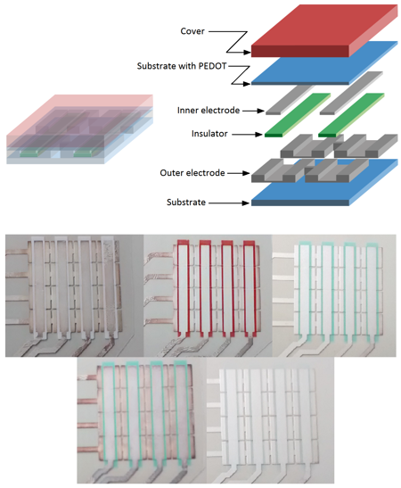
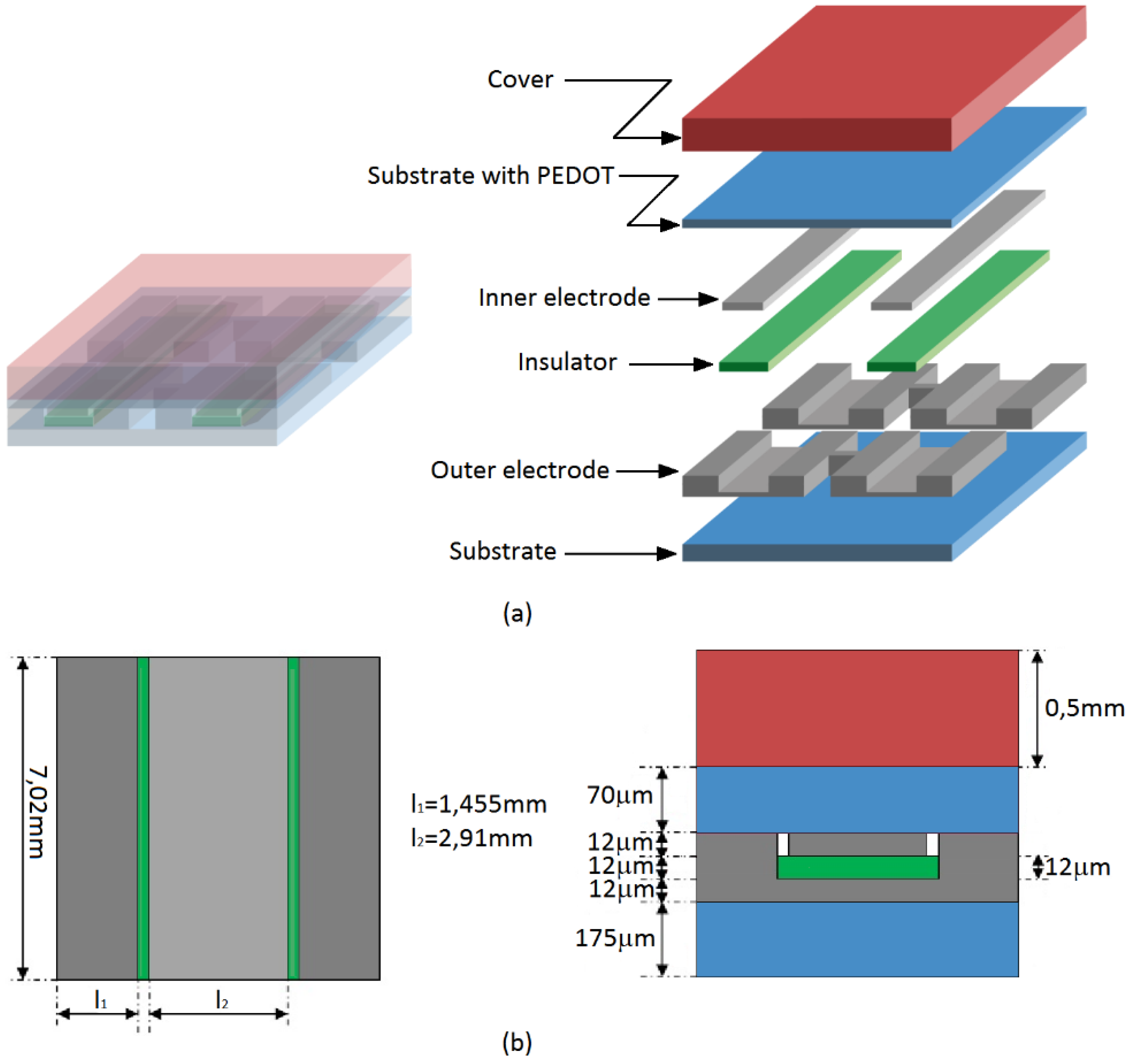
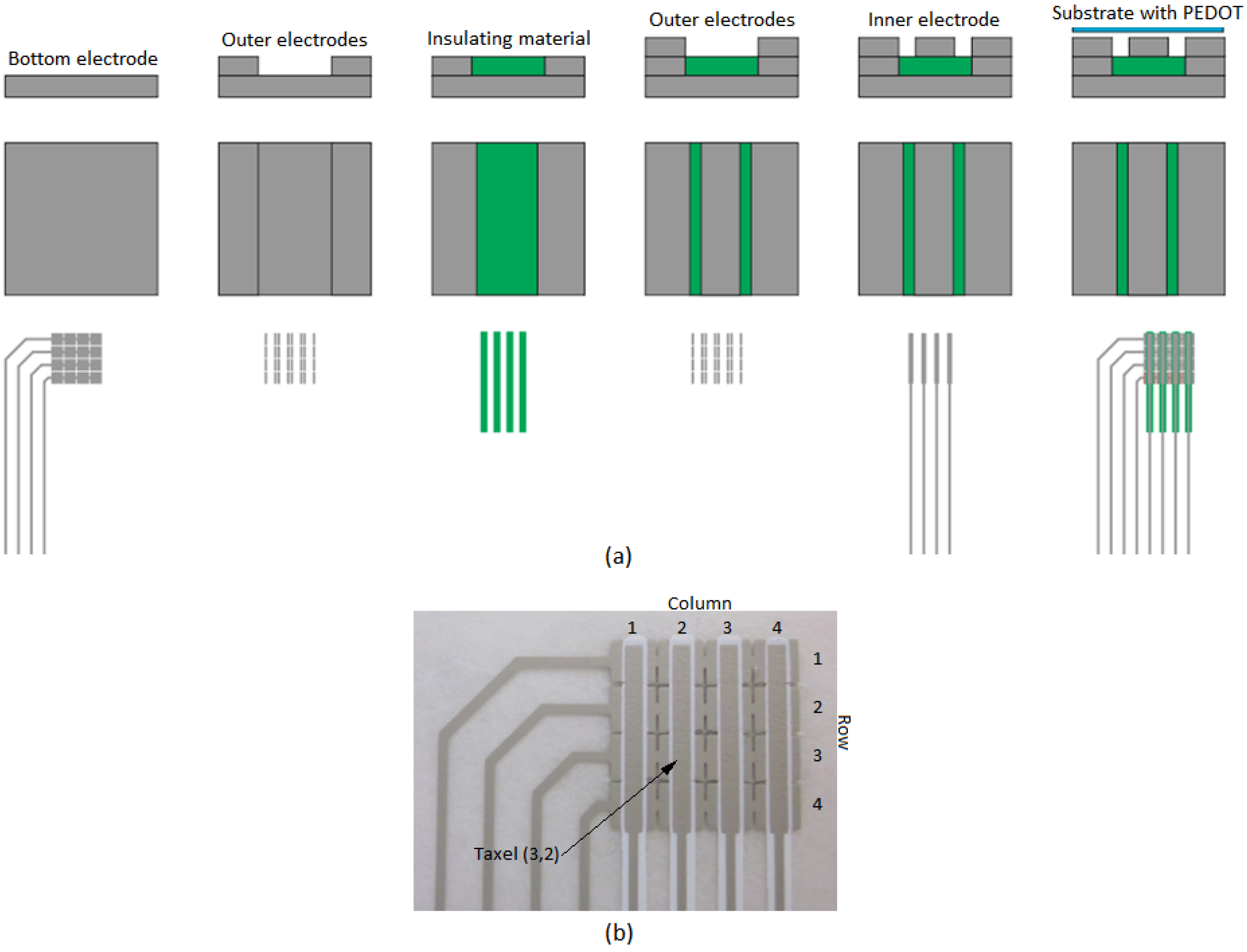
2. Design and Realization

- Initially, a silver conductive layer (bottom electrode) is deposited onto the 175 µm PET (polyethylene terephthalate) flexible plastic support and cured at 130 °C for 4 min in a natural convection oven (Carbolite PN 200).
- Another conductive layer is placed atop the bottom electrode, and cured again in the oven at 130 °C for 4 min.
- The insulating material is printed over it. The insulating materials have different thermal curing profiles.
- Another conductive layer is placed atop the bottom electrode, and cured again in the oven at 130 °C for 4 min (outer electrode).
- In the last screen printing step, the inner conductive electrode is deposited on the insulating material to reach the same height as the outer electrode.
- In the final step, a film of conductive polymer PEDOT is deposited by spin-coating on a 70 µm thick layer of PET. This layer is placed on top of the previous one with the PEDOT in contact with the electrodes.

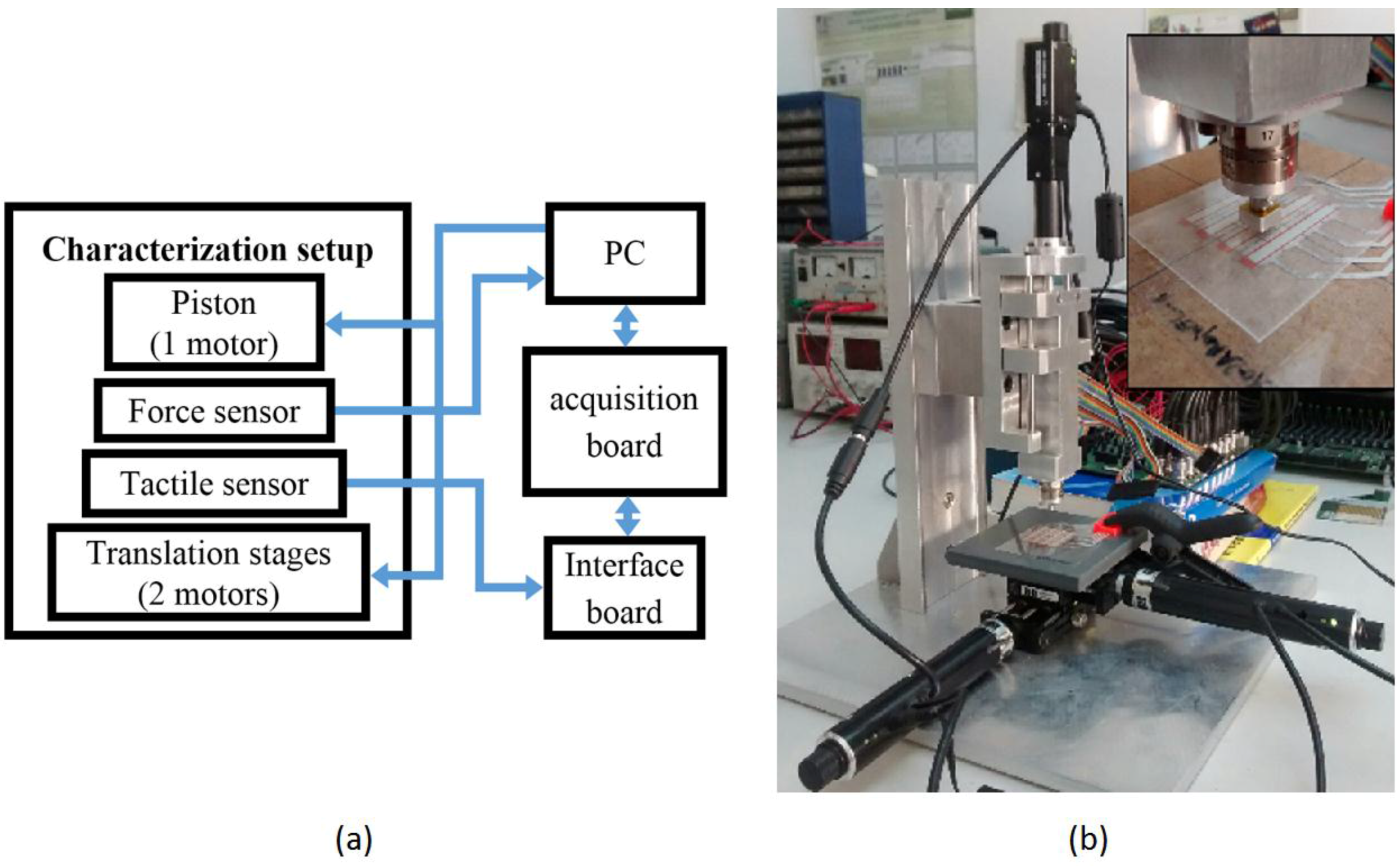
3. Experimental Setup
3.1. Setup to Test the Tactile Sensors

3.2. Young’s Modulus Estimation

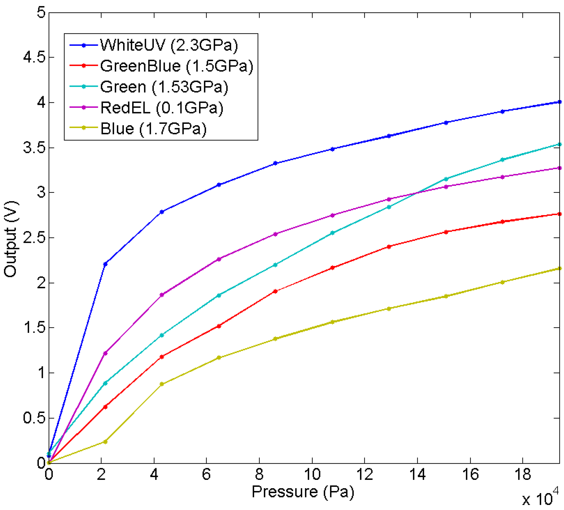
| Layer | Young’s Modulus (Pa) |
|---|---|
| Insulator WhiteUV | 2.3 × 10⁹ |
| Insulator Green | 1.53 × 10⁹ |
| Insulator GreenBlue | 1.5 × 10⁹ |
| Insulator RedEL | 0.1 × 10⁹ |
| Insulator Blue | 1.7 × 10⁹ |
| Insulator TranspUV | 3.3 × 10⁹ |
| Cover Pt | 0.14 × 10⁶ |
| Cover Red | 0.68 × 10⁶ |
| Cover Transp | 323.52 × 10⁶ |
| Cover PC | 1299 × 106 |
| Substrate (PET) | 2704.87 × 106 |
| Electrode | 2.96 × 10⁹ |
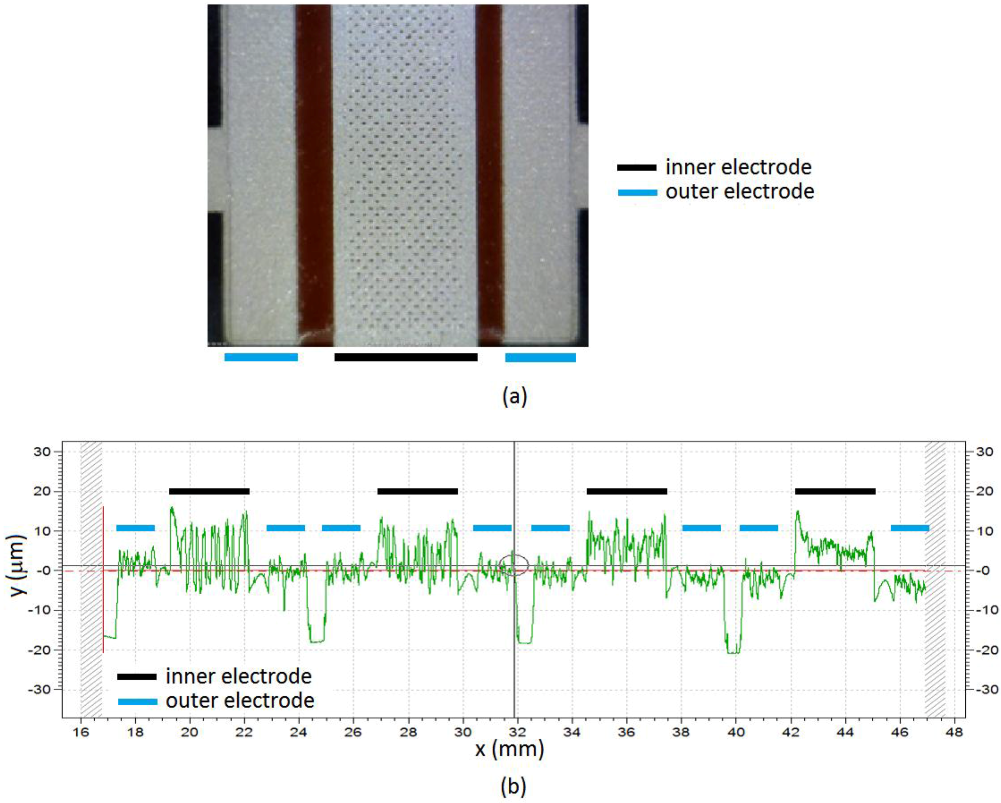
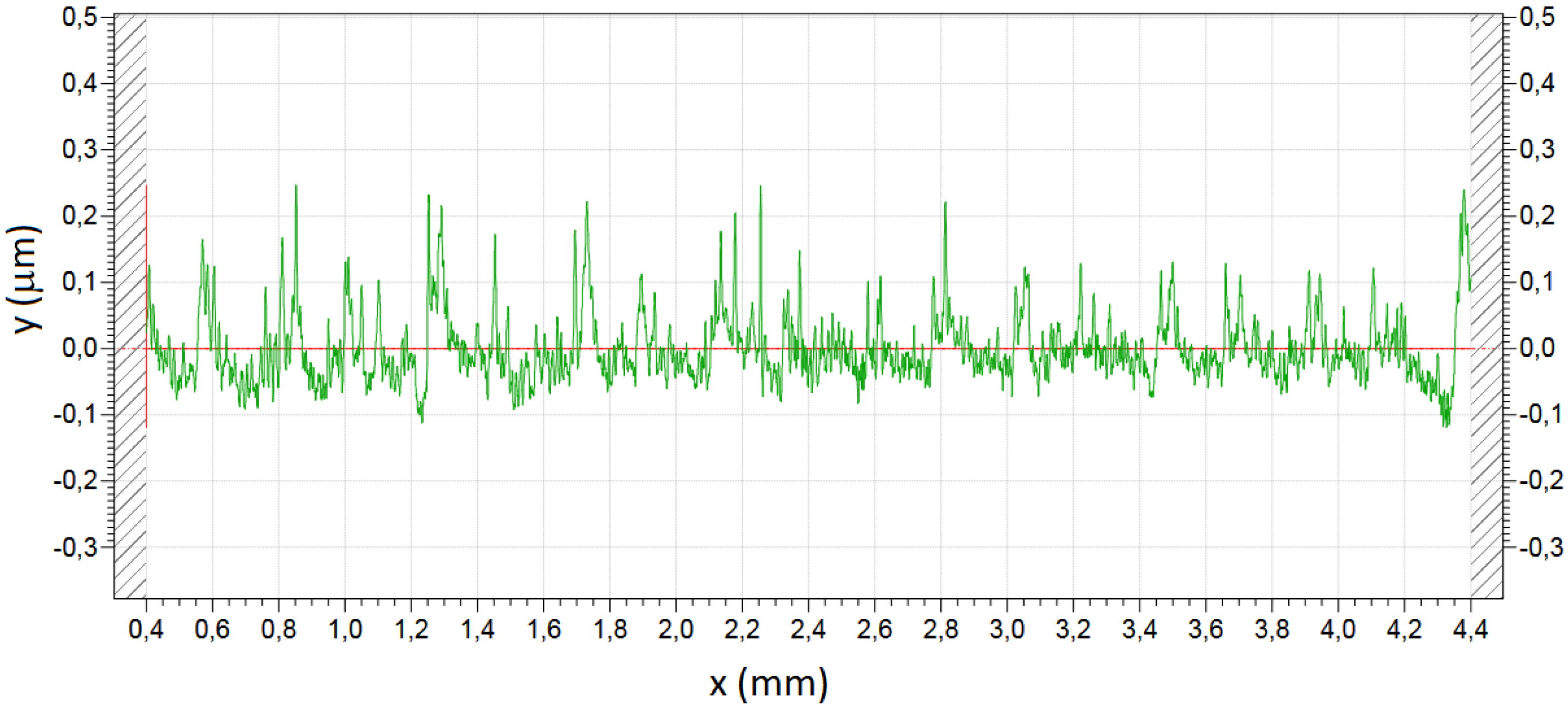
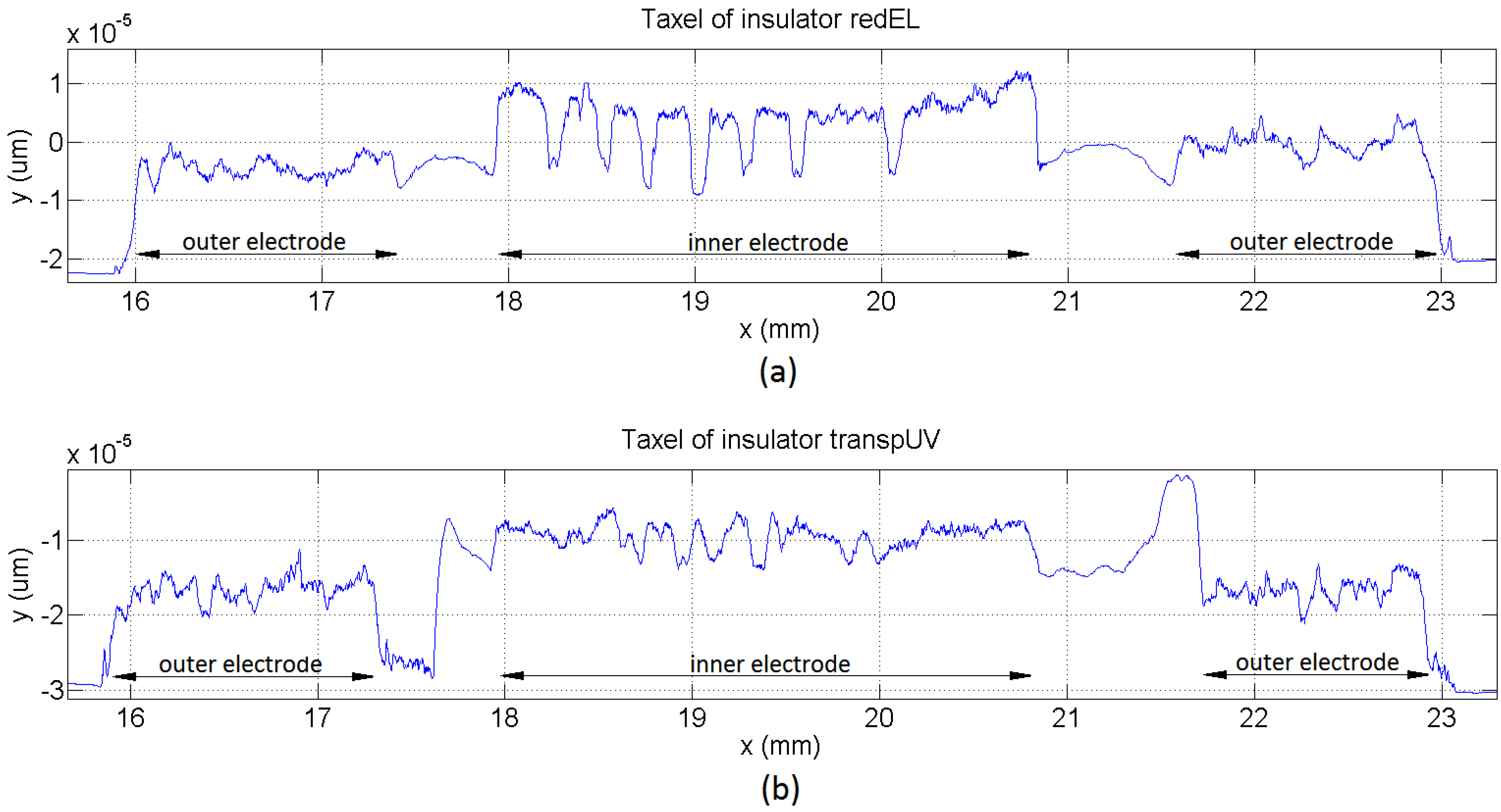
3.3. Profilometries
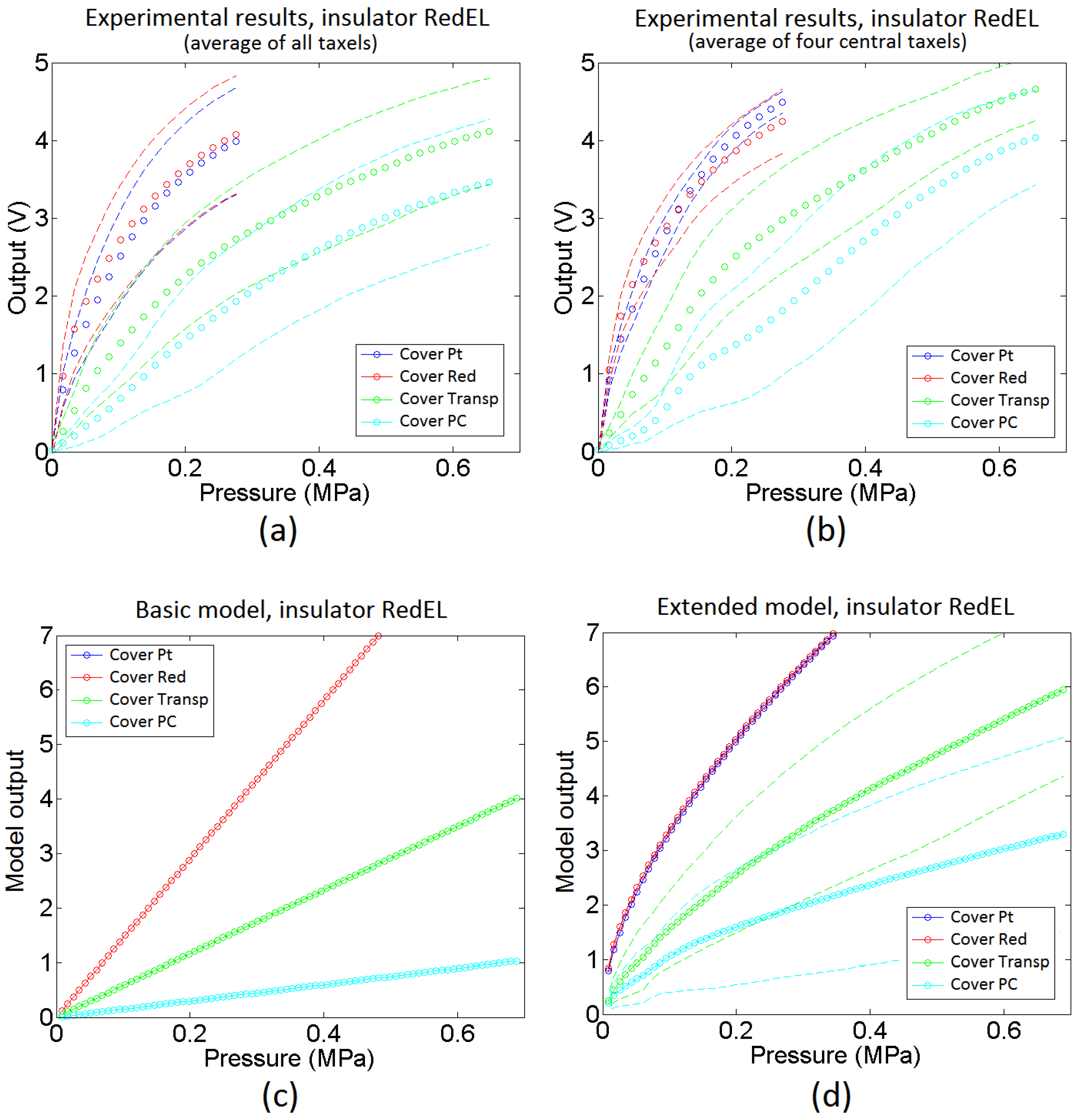
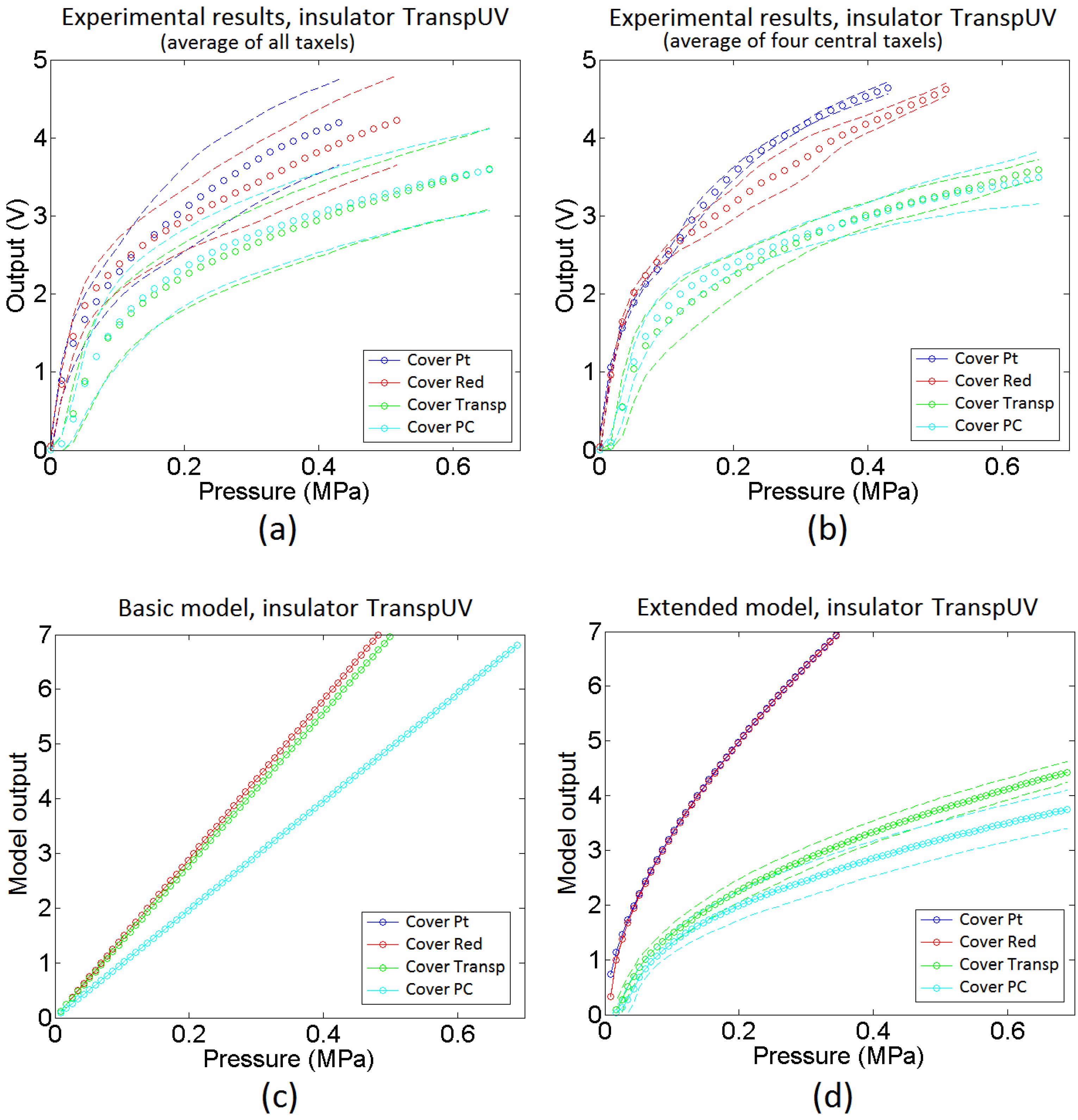
4. Analysis and Modelling of the Sensor Static Response
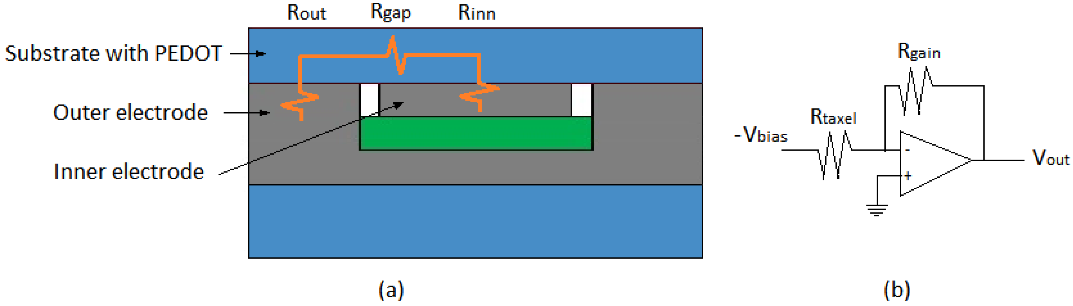
4.1. Basic Electrical Model

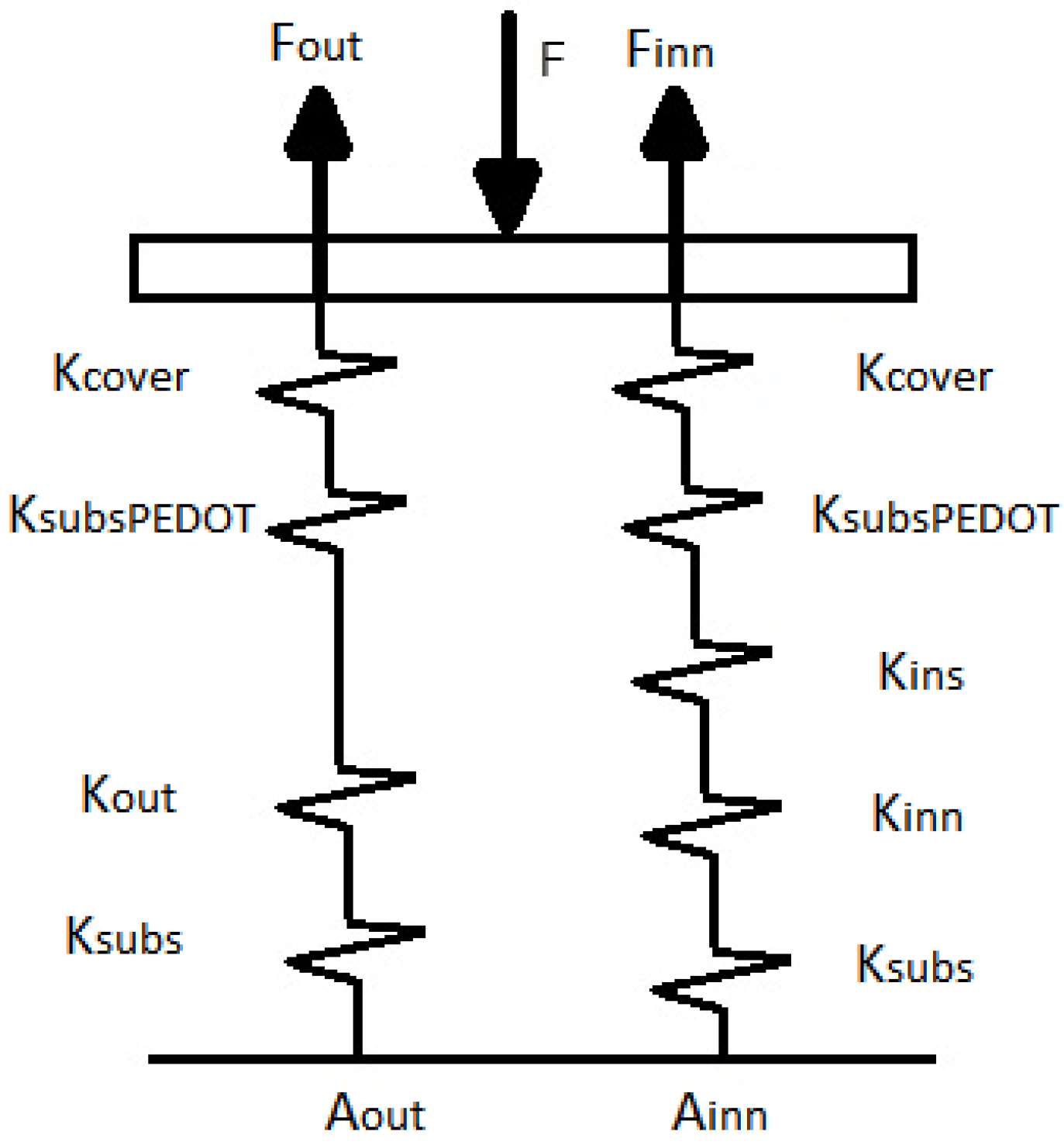
4.2. Basic Mechanical Model


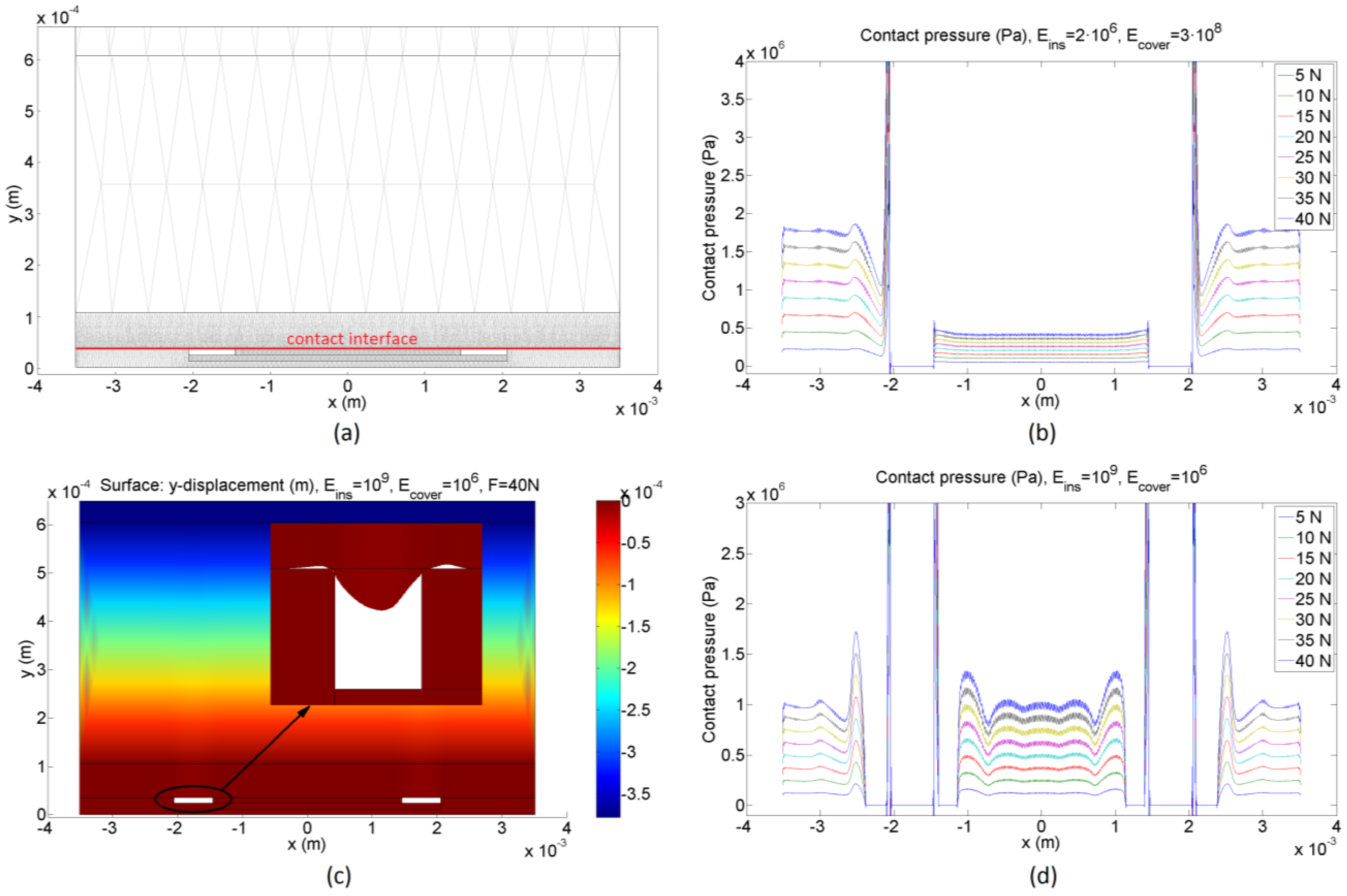
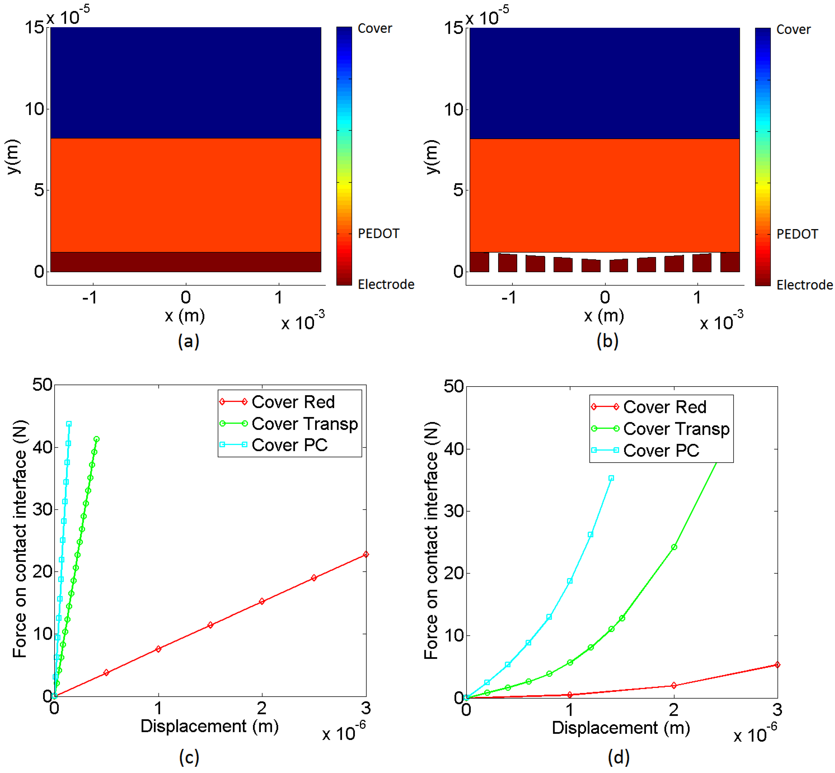
4.3. Finite Element Analysis
- The bottom boundary of the substrate has a fixed constraint condition.
- The lateral boundaries of the substrate, the polymer ink on plastic layer and the cover have a symmetry plane constrain condition.
- The top boundary of the aluminium plate has a free constraint condition and a load in the y axis direction.


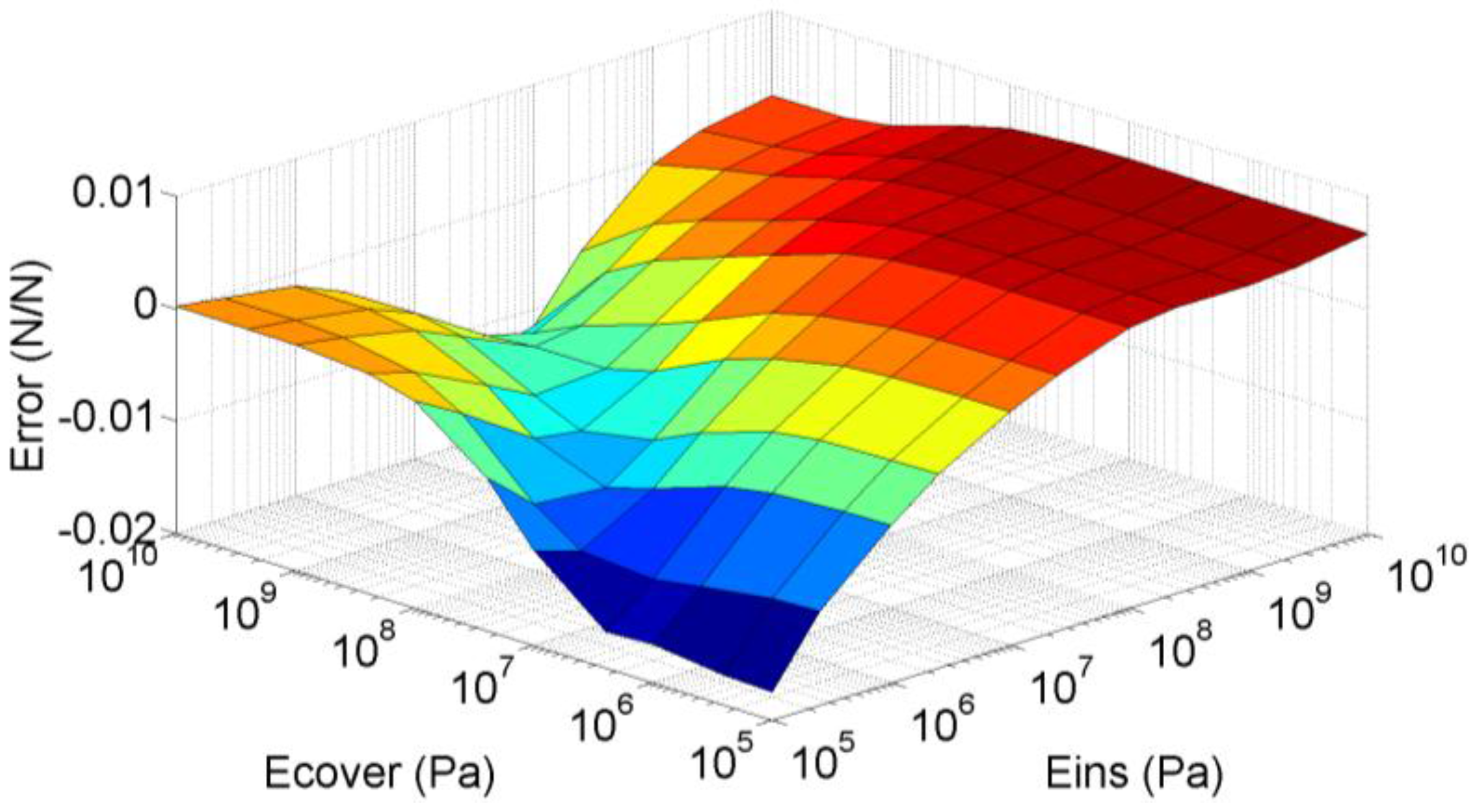
4.4. Limitations of the Simple Model
- The contacts are identical or at least the relationship between and in Equation (6) does not depend on .
- The force is distributed between both electrodes as stated in Equation (7), i.e. the total force on the taxel equals the summation of the forces on the electrodes.
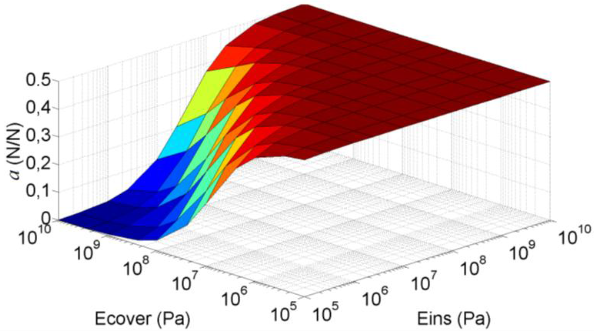
- The balance between the forces on both electrodes, i.e. the parameter a, does not depend on .
- The electrodes are flat and are at the same height.
- The pressure along the surface of the contacts is uniform.


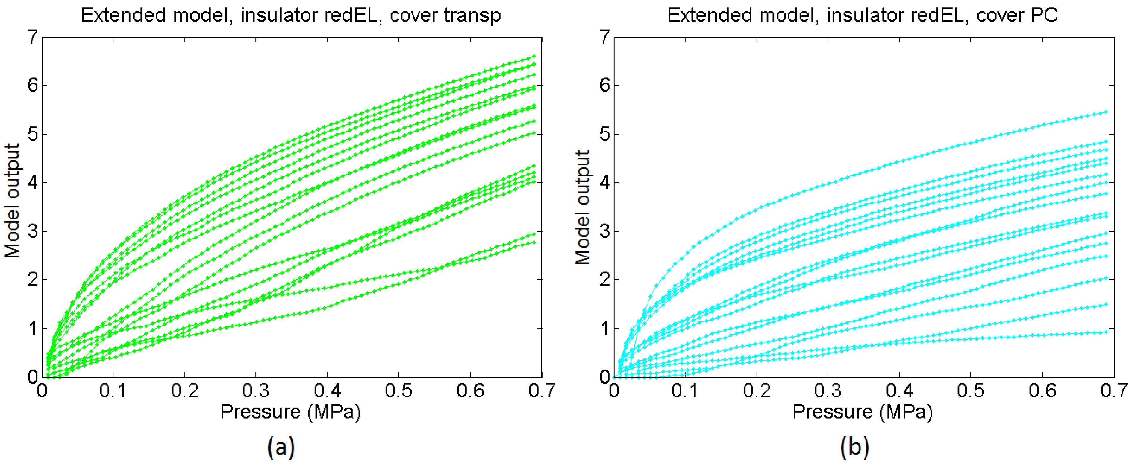
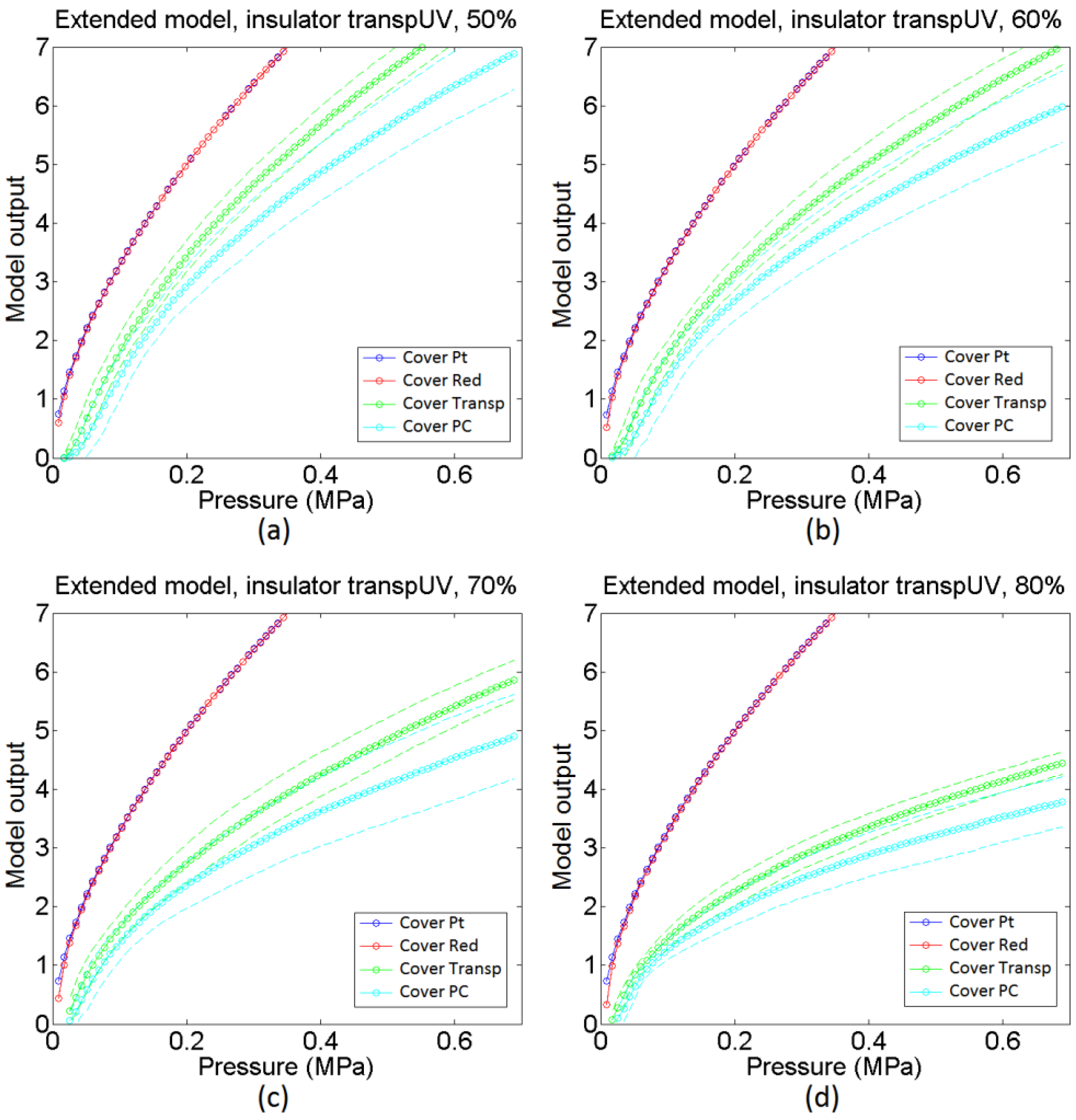
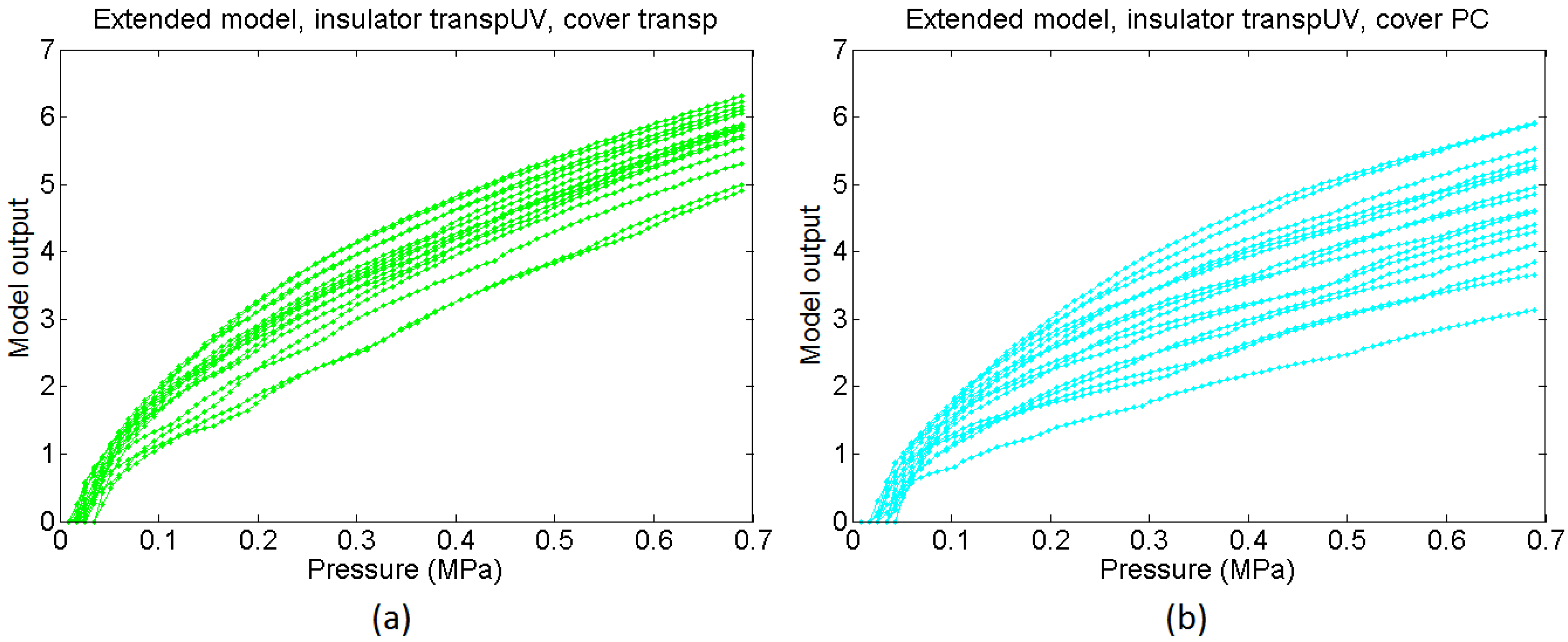
4.5. Extended Model

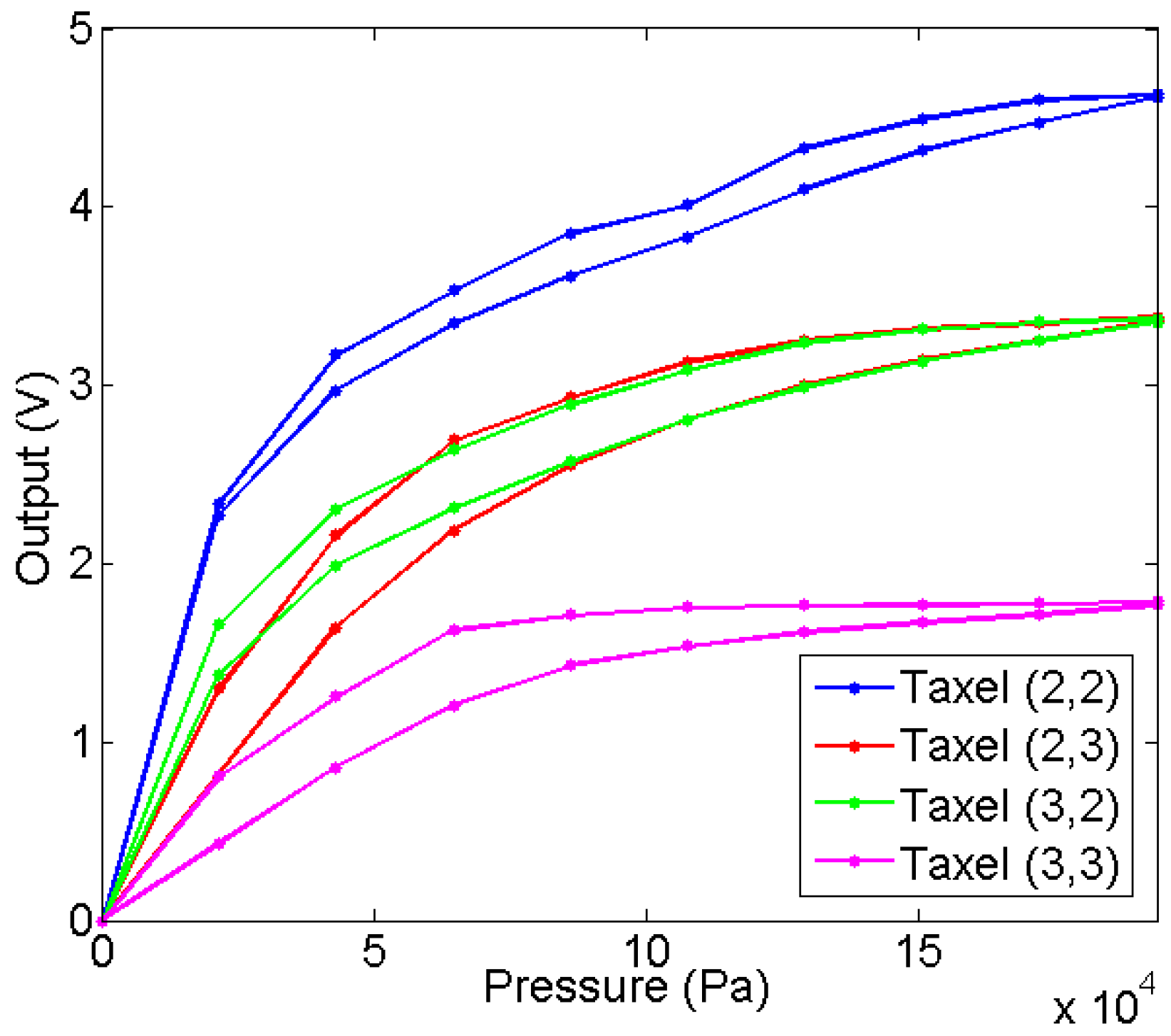
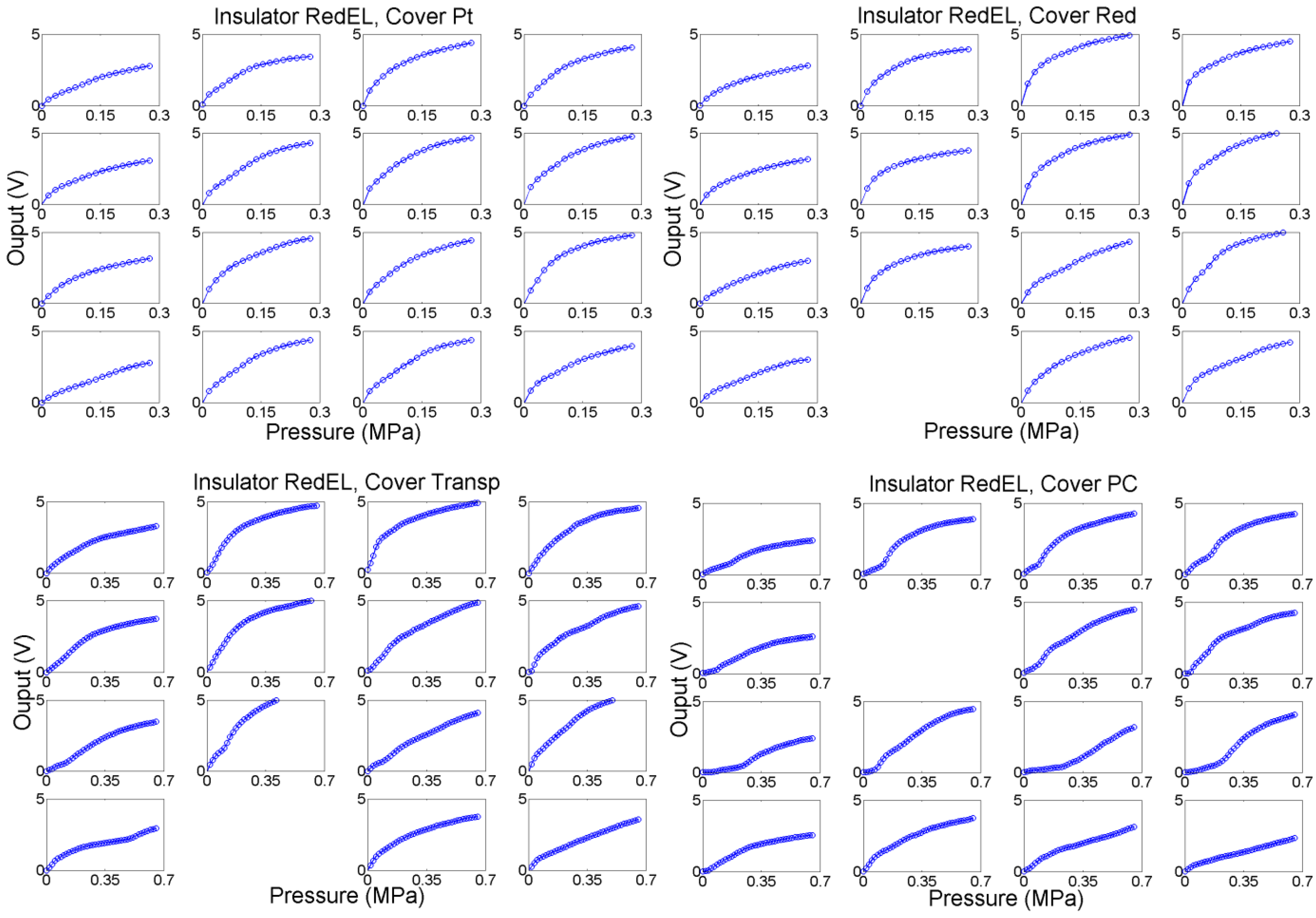
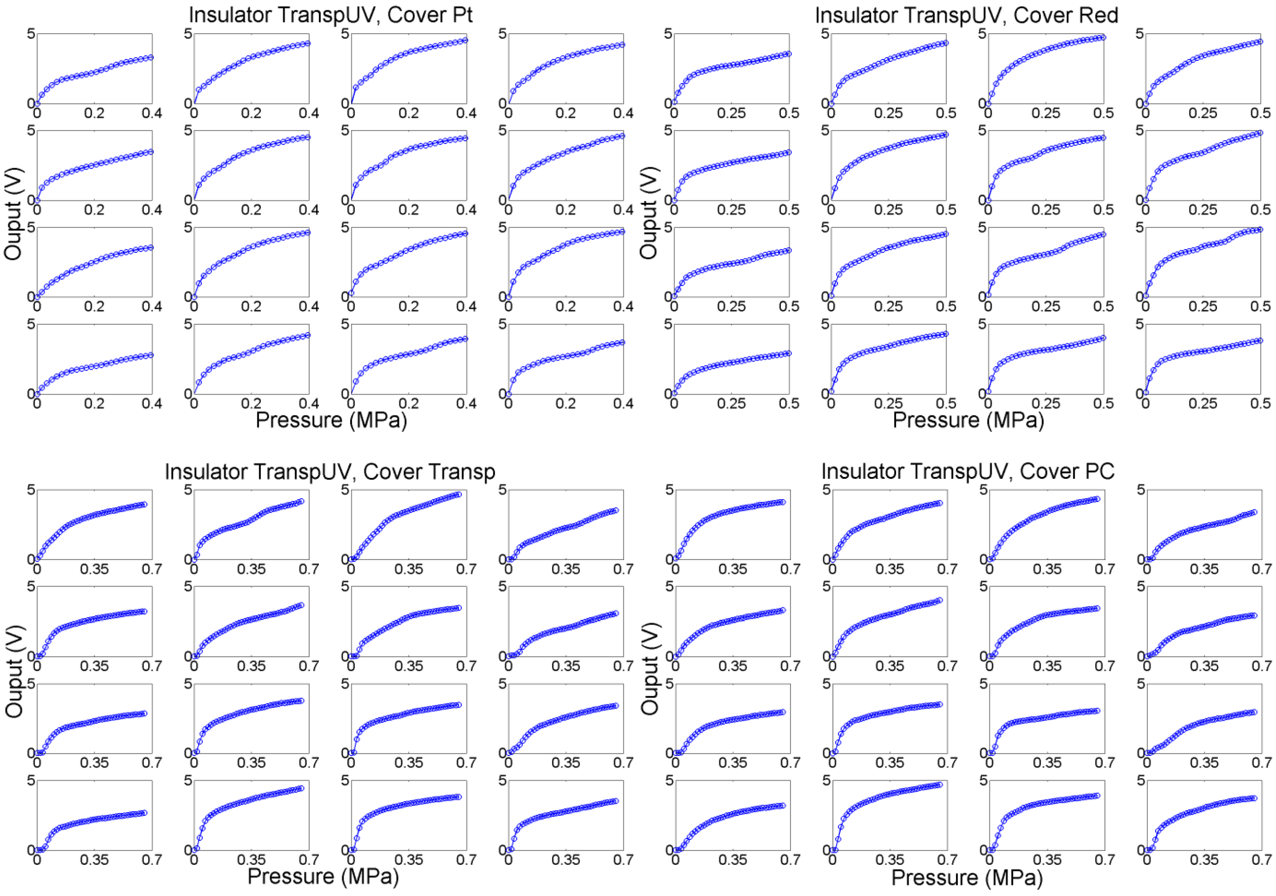
5. Experimental Results and Discussion


| Insulator | Cover | Hysteresis (%) | Area 2nd derivative (V/MPa) |
|---|---|---|---|
| RedEL | Pt | 14.03 | 36.90 |
| Red | 7.35 | 45.59 | |
| Tranps | 14.87 | 22.96 | |
| PC | 13.58 | 24.40 | |
| TranspUV | Pt | 15.27 | 49.66 |
| Red | 7.60 | 45.88 | |
| Transp | 13.58 | 51.59 | |
| PC | 11.68 | 48.01 |

6. Conclusions
Acknowledgments
Author Contributions
Conflicts of Interest
References
- Dahiya, R.S.; Metta, G.; Valle, M.; Sandini, G. Tactile Sensing-From Humans to Humanoids. IEEE Trans. Robot. 2010, 26, 1–20. [Google Scholar] [CrossRef]
- Engel, J.; Chen, J.; Fan, Z.; Liu, C. Polymer micromachined multimodal tactile sensors. Sens. Actuat. Phys. 2005, 117, 50–61. [Google Scholar] [CrossRef]
- Tactile Sensors and Pressure Mapping Solutions. Available online: http://www.pressureprofile.com/ (accessed on 1 August 2015).
- Lee, H.-K.; Chang, S.-I.; Yoon, E. A Flexible Polymer Tactile Sensor: Fabrication and Modular Expandability for Large Area Deployment. J. Microelectromech. Syst. 2006, 15, 1681–1686. [Google Scholar] [CrossRef]
- Cannata, G.; Maggiali, M.; Metta, G.; Sandini, G. An embedded artificial skin for humanoid robots. In Proceedings of the 2008 IEEE International Conference on Multisensor Fusion and Integration for Intelligent Systems, Seoul, Korea, 20–22 August 2008; pp. 434–438.
- Hussain, M.; Choa, Y.-H.; Niihara, K. Conductive rubber materials for pressure sensors. J. Mater. Sci. Lett. 2001, 20, 525–527. [Google Scholar] [CrossRef]
- Drimus, A.; Jankovics, V.; Gorsic, M.; Matefi-Tempfli, S. Novel high resolution tactile robotic fingertips. In Proceedings of the 2014 IEEE SENSORS, Valencia, Spain, 2–5 November 2014; pp. 791–794.
- Cannata, G.; Maggiali, M. An embedded tactile and force sensor for robotic manipulation and grasping. In Proceedings of the 2005 5th IEEE-RAS International Conference on Humanoid Robots, Tsukuba, Japan, 5–7 December 2005; pp. 80–85.
- Kobayashi, K.; Ito, N.; Mizuuchi, I.; Okada, K.; Inaba, M. Design and realization of fingertiped and multifingered hand for pinching and rolling minute objects. In Proceedings of the 9th IEEE-RAS International Conference on Humanoid Robots, Paris, France, 7–10 December 2009; pp. 263–268.
- QTCTM Material Technology. Available online: http://www.peratech.com/qtc-technology.html (accessed on 11 September 2015).
- Wang, L.; Ding, T.; Wang, P. Thin Flexible Pressure Sensor Array Based on Carbon Black/Silicone Rubber Nanocomposite. IEEE Sens. J. 2009, 9, 1130–1135. [Google Scholar] [CrossRef]
- Franklin, N. Eventoff Electronic pressure sensitive transducer apparatus. US4,314,227 A, 2 February 1982. [Google Scholar]
- Papakostas, T.V.; Lima, J.; Lowe, M. A large area force sensor for smart skin applications. In Proceedings of the 2002 IEEE Sensors, Orlando, FL, USA, 12–14 June 2002; pp. 1620–1624.
- Strohmayr, M.W.; Worn, H.; Hirzinger, G. The DLR artificial skin step I: Uniting sensitivity and collision tolerance. In Proceedings of the 2013 IEEE International Conference on Robotics and Automation (ICRA), Karlsruhe, Germany, 6–10 May 2013; pp. 1012–1018.
- Tekscan | Pressure Mapping, Force Measurement, & Tactile Sensors. Available online: https://www.tekscan.com/ (accessed on 1 August 2015).
- Interlink Electronics. Available online: http://www.interlinkelectronics.com/resistive.php (accessed on 11 September 2015).
- Sensitronics. Available online: http://www.sensitronics.com/products.php (accessed on 11 September 2015).
- Jockusch, J.; Walter, J.; Ritter, H. A tactile sensor system for a three-fingered robot manipulator. In Proceedings of the 1997 IEEE International Conference on Robotics and Automation, Albuquerque, NM, USA, 20–25 April 1997; pp. 3080–3086.
- Schmidt, P.A.; Maël, E.; Würtz, R.P. A sensor for dynamic tactile information with applications in human–robot interaction and object exploration. Robot. Auton. Syst. 2006, 54, 1005–1014. [Google Scholar] [CrossRef]
- Kalamdani, A.; Messom, C.; Siegel, M. Tactile Sensing by the Sole of the Foot Part II: Calibration and Real-time Processing. In Proceedings of the 3rd International Conference on Autonomous Robots and Agents, Palmerston North, New Zealand, 12–14 December 2006.
- Hartmann, J.M.; Rudert, M.J.; Pedersen, D.R.; Baer, T.E.; Goreham-Voss, C.M.; Brown, T.D. Compliance-dependent load allocation between sensing versus non-sensing portions of a sheet-array contact stress sensor. Iowa Orthop. J. 2009, 29, 43–47. [Google Scholar] [PubMed]
- Weiss Robotics GmbH & Co. KG. Available online: http://www.weiss-robotics.de/en/ (accessed on 15 September 2015).
- Göger, D.; Gorges, N.; Worn, H. Tactile sensing for an anthropomorphic robotic hand: Hardware and signal processing. In Proceedings of the IEEE International Conference on Robotics and Automation, Kobe, Japan, 12 May 2009; pp. 895–901.
- Castellanos-Ramos, J.; Navas-González, R.; Macicior, H.; Sikora, T.; Ochoteco, E.; Vidal-Verdú, F. Tactile sensors based on conductive polymers. Microsyst. Technol. 2010, 16, 765–776. [Google Scholar] [CrossRef]
- Greenwood, J.A. Constriction resistance and the real area of contact. Br. J. Appl. Phys. 1966, 17, 1621–1632. [Google Scholar] [CrossRef]
- Barber, J.R. Incremental stiffness and electrical contact conductance in the contact of rough finite bodies. Phys. Rev. E 2013, 87. [Google Scholar] [CrossRef]
- Pastewka, L.; Prodanov, N.; Lorenz, B.; Müser, M.H.; Robbins, M.O.; Persson, B.N.J. Finite-size scaling in the interfacial stiffness of rough elastic contacts. Phys. Rev. E 2013, 87. [Google Scholar] [CrossRef] [Green Version]
- Liu, T.; Inoue, Y.; Shibata, K. A Small and Low-Cost 3-D Tactile Sensor for a Wearable Force Plate. IEEE Sens. J. 2009, 9, 1103–1110. [Google Scholar] [CrossRef]
- Yang, Y.-J.; Cheng, M.-Y.; Shih, S.-C.; Huang, X.-H.; Tsao, C.-M.; Chang, F.-Y.; Fan, K.-C. A 32 × 32 temperature and tactile sensing array using PI-copper films. Int. J. Adv. Manuf. Technol. 2009, 46, 945–956. [Google Scholar] [CrossRef]
- Weiss, K.; Worn, H. The working principle of resistive tactile sensor cells. In Proceedings of the 2005 IEEE International Conference on Mechatronics and Automation, Niagara Falls, Canada, 29 July–1 August 2005; pp. 471–476.
- THIEME 1000E. Available online: http://www.thieme.eu/en/thieme-1000e-screen-printing-machine (accessed on 1 August 2015).
- Taylor Hobson, Surface Profilers | Surface Profiliometer. Available online: http://www.taylor-hobson.com/products/13/107.html (accessed on 1 August 2015).
- Barber, J.R. Bounds on the electrical resistance between contacting elastic rough bodies. Proc. R. Soc. Lond. Math. Phys. Eng. Sci. 2003, 459, 53–66. [Google Scholar] [CrossRef]
- Greenwood, J.A.; Williamson, J.B.P. Contact of Nominally Flat Surfaces. Proc. R. Soc. Lond. Math. Phys. Eng. Sci. 1966, 295, 300–319. [Google Scholar] [CrossRef]
- Lorenz, B.; Persson, B.N.J. Interfacial separation between elastic solids with randomly rough surfaces: comparison of experiment with theory. J. Phys. Condens. Matter 2009, 21. [Google Scholar] [CrossRef] [PubMed]
- Castellanos-Ramos, J.; Navas-González, R.; Ochoteco, E.; Vidal-Verdú, F. Finite element analysis of tactile sensors made with screen printing technology. In Proceedings of the SPIE 8068, Bioelectronics, Biomedical, and Bioinspired Systems V; and Nanotechnology, Prague, Czech Republic, 18–20 April 2011; pp. 806804–1–806804–10.
- Hyun, S.; Pei, L.; Molinari, J.-F.; Robbins, M.O. Finite-element analysis of contact between elastic self-affine surfaces. Phys. Rev. E 2004, 70. [Google Scholar] [CrossRef]
- Ciavarella, M.; Murolo, G.; Demelio, G.; Barber, J.R. Elastic contact stiffness and contact resistance for the Weierstrass profile. J. Mech. Phys. Solids 2004, 52, 1247–1265. [Google Scholar] [CrossRef]
- Ciavarella, M.; Dibello, S.; Demelio, G. Conductance of rough random profiles. Int. J. Solids Struct. 2008, 45, 879–893. [Google Scholar] [CrossRef]
- Pohrt, R.; Popov, V.L. Normal Contact Stiffness of Elastic Solids with Fractal Rough Surfaces. Phys. Rev. Lett. 2012, 108. [Google Scholar] [CrossRef]
- Harada, K.; Tsuji, T.; Uto, S.; Yamanobe, N.; Nagata, K.; Kitagaki, K. Stability of soft-finger grasp under gravity. In Proceedings of the 2014 IEEE International Conference on Robotics and Automation (ICRA), Hong Kong, China, 31 May–7 June 2014; pp. 883–888.
- Nobili, A. Variational Approach to Beams Resting on Two-Parameter Tensionless Elastic Foundations. J. Appl. Mech. 2012, 79. [Google Scholar] [CrossRef]
- Archard, J.F. Elastic Deformation and the Laws of Friction. Proc. R. Soc. Lond. Ser. Math. Phys. Sci. 1957, 243, 190–205. [Google Scholar] [CrossRef]
- Greenwood, J.A.; Wu, J.J. Surface Roughness and Contact: An Apology. Meccanica 2001, 36, 617–630. [Google Scholar] [CrossRef]
- Ciavarella, M.; Delfine, V.; Demelio, G. A “re-vitalized” Greenwood and Williamson model of elastic contact between fractal surfaces. J. Mech. Phys. Solids 2006, 54, 2569–2591. [Google Scholar] [CrossRef]
© 2015 by the authors; licensee MDPI, Basel, Switzerland. This article is an open access article distributed under the terms and conditions of the Creative Commons Attribution license (http://creativecommons.org/licenses/by/4.0/).
Share and Cite
Castellanos-Ramos, J.; Navas-González, R.; Fernández, I.; Vidal-Verdú, F. Insights into the Mechanical Behaviour of a Layered Flexible Tactile Sensor. Sensors 2015, 15, 25433-25462. https://doi.org/10.3390/s151025433
Castellanos-Ramos J, Navas-González R, Fernández I, Vidal-Verdú F. Insights into the Mechanical Behaviour of a Layered Flexible Tactile Sensor. Sensors. 2015; 15(10):25433-25462. https://doi.org/10.3390/s151025433
Chicago/Turabian StyleCastellanos-Ramos, Julián, Rafael Navas-González, Iván Fernández, and Fernando Vidal-Verdú. 2015. "Insights into the Mechanical Behaviour of a Layered Flexible Tactile Sensor" Sensors 15, no. 10: 25433-25462. https://doi.org/10.3390/s151025433