Reactive Sputtering of Aluminum Nitride (002) Thin Films for Piezoelectric Applications: A Review


Queensland Micro- and Nanotechnology Centre, Griffith University, Nathan, QLD 4111, Australia
*
Author to whom correspondence should be addressed.
Sensors 2018, 18(6), 1797; https://doi.org/10.3390/s18061797
Submission received: 24 April 2018
/
Revised: 31 May 2018
/
Accepted: 1 June 2018
/
Published: 2 June 2018
(This article belongs to the Section Physical Sensors)
Abstract
:We summarize the recipes and describe the role of sputtering parameters in producing highly c-axis Aluminum Nitride (AlN) films for piezoelectric applications. The information is collated from the analysis of around 80 journal articles that sputtered this film on variety of substrate materials, processes and equipment. This review will be a good starting point to catch up with the state-of-the-arts research on the reactive sputtering of AlN (002) thin film, as well as its evolving list of piezoelectric applications such as energy harvesters.
1. Introduction
Energy harvesting or energy scavenging is the process of extracting energy from the ambient sources in the environment. Energy harvester, instead of battery usage, is preferred for powering wireless sensors because the latter is limited by its limited life span. The ambient sources are broadly divided into four categories: Solar, thermal, wind, and mechanical vibration [1]. Researchers have investigated different methods to convert them into electrical energy via resonant and non-resonant devices [2]. A variety of transduction schemes have been proposed using solar, thermoelectric, electromagnetic, piezoelectric, capacitive etc. Among them, piezoelectric emerges as one of the most practical solutions. It does not require external power sources for polarization in comparison to the electrostatic transductions. Furthermore, the micro-scale fabrication processes are simpler compared to the electromagnetic transductions [3].
Piezoelectricity is derived from the Greek word “piezo”, which means “to squeeze”. It is the property of the crystalline materials that develop an electric dipole when the mechanical strain is applied to them. Conversely, they exhibit an induced mechanical strain when being subjected to an electric potential. In dielectrics, the electrons are strongly tied to the outermost atomic shells and form a symmetrical cloud around the nucleus in the absence of an electric field. In the non-polar dielectric, the electric field polarizes the atom or the molecules in the material by moving the center of the electron cloud away from the nucleus, resulting in the formation of an electric dipole. All of these individual dipoles add up over the entire crystal and produce the net polarization that results in electric field generation across the material [4].
Figure 1 shows the block diagram to convert the mechanical to the electrical energies using piezoelectric transduction. There are three major steps. First, the mechanical energy is absorbed from the ambient environment. It can be in the form of vibration, force, or motion. Then, this energy is piezo-electrically transduced to electrical voltage and current. Finally, the electrical energy is rectified and stored [5].
Piezoelectric materials are classified as single crystal, polycrystalline, polymers, ceramics, and thin films. The selection of the most suitable forms depends on the availability of the deposition methods, the process complexities, and their compatibility with the targeted applications. Thin films have a substantial range of advantages such as low hysteresis, high sensitivity, low power requirements, and the ability to generate large mechanical deflections. The three most commonly used piezoelectric thin films are lead zirconate titanate (PZT), zinc oxide (ZnO), and aluminum nitride (AlN).
PZT film is preferred in piezoelectric applications due to its high electromechanical coupling coefficient (k2) and piezoelectric coefficient (dij). However, the presence of lead in this material results in higher probability of contamination in the clean room during its processing. ZnO and AlN possess similar values of k2 and dij. However, the performance of ZnO degrades significantly at high temperature due to its low Curie point. As a result, AlN trumps ZnO in the fabrication of the micro-scale piezoelectric devices at such temperature.
AlN thin films can be produced via various methods including metal organic chemical vapor deposition (MOCVD), molecular beam epitaxy (MBE), electron cyclotron resonance dual-ion beam sputtering, and pulsed laser ablation. However, these methods are expensive and the high processing temperatures are required. Direct current (DC) and radio frequency (RF) sputtering have the advantages of being low temperature and low-cost, making them suitable for the fabrication of Micro-Electro-Mechanical Systems (MEMS) devices.
Amongst MEMS applications, many groups are looking at AlN thin films to make piezoelectric energy harvesters. This development makes the review of the latest published works on the sputtering of AlN thin film timely. The information has been collated from around 80 articles that were published in well-known thin film journals. We would like to acknowledge that Iriarte et al. wrote a review article that detailed the sputtering parameters that influence the formation of c-axis AlN film in 2010 [6]. In order to produce definitive trends, they used pulsed DC sputtering to deposit AlN films on a variety of substrates such as Si, quartz, AlO2, MgO, MgAl2O4, and diamond. They did not however compile a list of sputtering recipes from other researchers. Therefore, we will provide those information. We would also like to state that this review only covers reactive sputtering of hexagonal AlN structures. Even though there are several works on the sputtering of cubic AlNs, we do not cover them here.
The rest of the paper is as follows. Section 2 describes the AlN crystal structure. Then, Section 3 lists some of the structural, optical, thermal, and piezoelectric properties of AlN. After that, Section 4 describes the basic sputtering process for AlN film for the benefit of the non-experts. Advanced users should skip this section. Section 5 is the “meat” of this review. It contains the table that summarizes all the recipes from the journal articles. The rest of that section describes the roles of sputtering parameters towards producing highly c-axis AlN films. Several articles also discussed the piezoelectric applications, for examples surface acoustic wave devices [7], bulk acoustic wave devices [8], and energy harvesters [9]. Section 6 concludes by emphasizing the inter-dependency of those parameters towards depositing the highly c-axis films.
2. AlN Crystal Structure
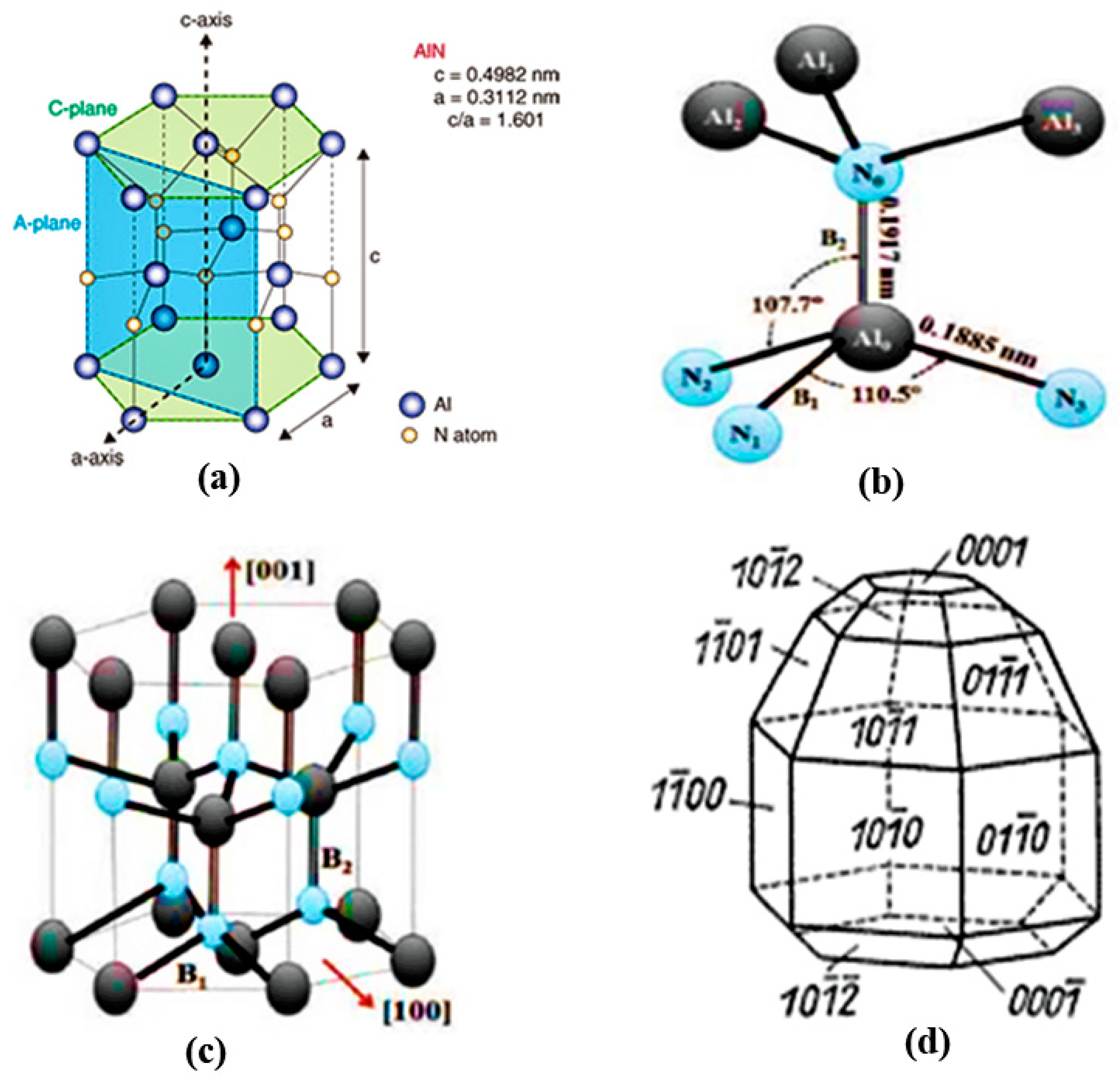
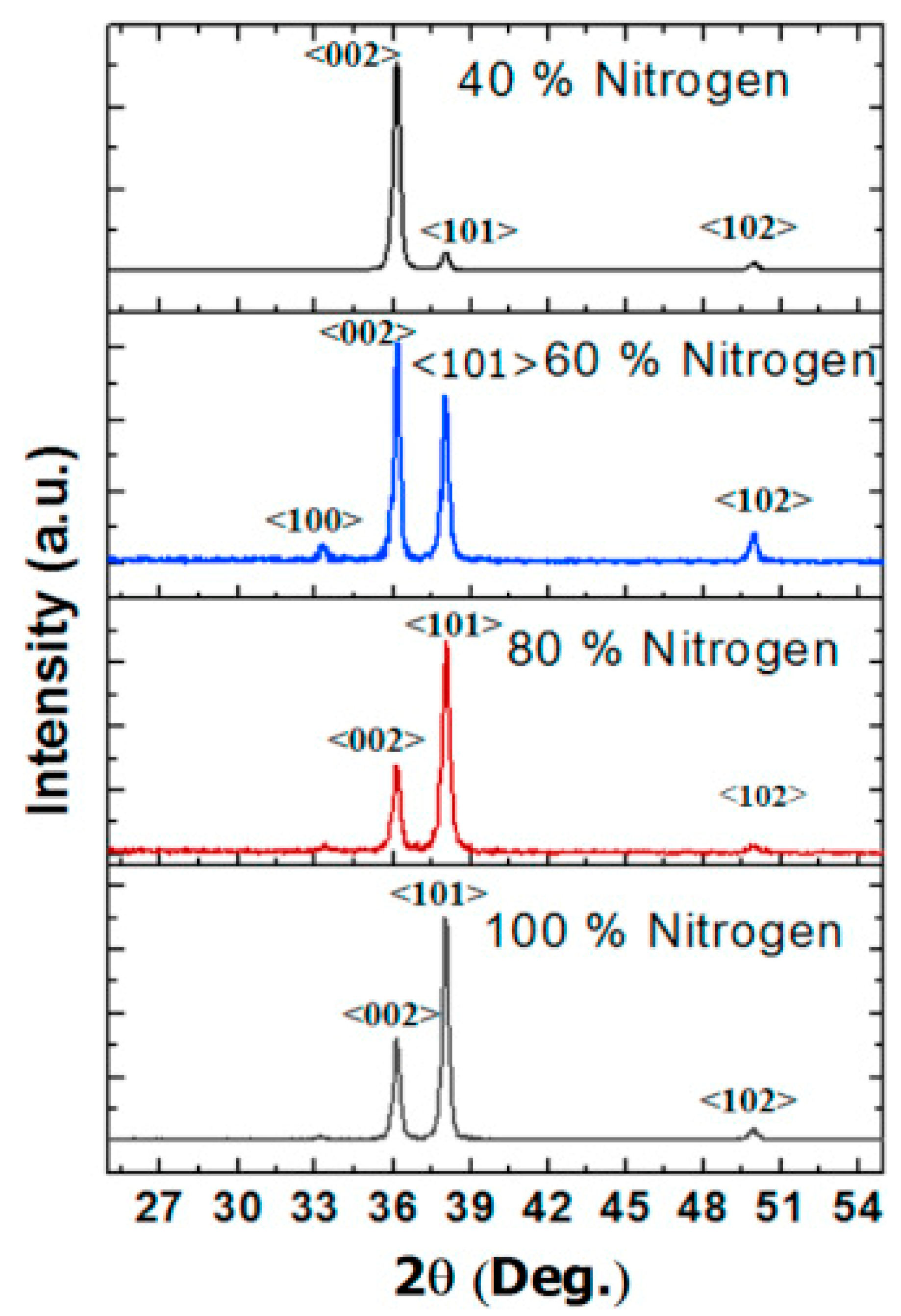
AlN belongs to group III–V semiconductor family because it has a hexagonal closed-packed wurtzite structure [10]. The lattice parameters range from 3.110 to 3.113 Å for the a-axis, and from 4.978 to 4.982 Å for the c-axis. The c/a ratio varies between 1.600 and 1.602. This deviation from the ideal wurtzite structure is credited to its lattice instability [11]. Figure 2 shows its crystalline structure, bonds configuration, and different planes. Each Al atom is surrounded by four N atoms to form a tetrahedron with three B1 bonds between Al-N(i=1,2,3) and one B2 bond between Al-N0 bond. The bond lengths of B1 and B2 are 0.1885 and 0.1917 nm, respectively. The bond angles for N0-Al-N1 and N1-Al-N2 are 107.7° and 110.5°, respectively. The (100) plane is composed of the B1 bonds, while the (002) and (101) planes consist of the B1 and B2 bonds [12]. Figure 3 shows the example of XRD plot of AlN films. This is taken from one of authors’ own article [8]. The 2θ peak positions for the (100), (101), (102), and (002) planes are clearly labeled. For example, the peak for (002) plane is at 2θ of 36°.
3. AlN Properties
Some of the structural, optical, thermal, and piezoelectric properties of bulk AlN are given in Table 1. These data are taken from references [13,14]. It should be clear that these data are not comprehensive, and there are a lot more mechanical and corrosion properties that we do not cover in Table 1. AlN has a large energy band-gap of 6.2 eV, a high thermal conductivity of 180 W/(m·°K), a high breakdown voltage of 1.2 × 10⁶ V/cm, and a high resistivity of 1015 Ohm·cm. It also has a high surface acoustic Wave (SAW) velocity of 12,000 m/s and a moderate k2 of ~1% [15]. The value of the latter parameter is highest along the (002) plane, prompting piezoelectric researchers to target for the production of a highly c-axis AlN film. Furthermore, AlN has higher values of mechanical, thermal and chemical stability compared to the other members of the III-V nitride semiconductors. Later in Section 5, we will highlight few works that sputtered AlN films and characterized their performances at those conditions.
4. Overview of Sputtering Process
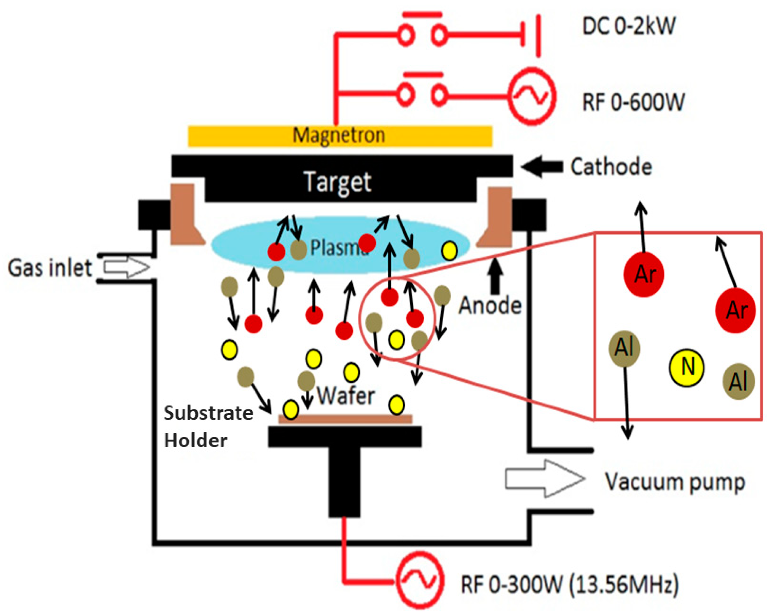
The generic sputtering process for AlN film is shown in Figure 4. This section is specifically written for non-experts, so that they could follow the discussions on the sputtering parameters in Section 5. The system consists of a chamber, gas inlet, vacuum pump, and power supply. The chamber houses the sputtering target and its shutter at the top, and wafer holder (or sometimes referred to as susceptor) at the bottom. The inlet feeds Argon (Ar) and Nitrogen (N2) gasses. The pump maintains the high vacuum condition in the chamber. The power supply could be DC, RF, or both. It feeds high voltage to the magnetron system that transmits electromagnetic waves from the cathode to the anode ring. In that process, the gasses inside the chamber are transformed into their plasma state. Initially, Ar is fed into the chamber through the inlet and gets ionized. After that, N2 is fed, undergoing the same transformation. Based on selection of the power supply, three sputtering modes could be set, namely reactive DC, reactive pulsed DC, and reactive RF modes. Suppose that we use reactive DC mode. The positive and negative potentials are applied to the anode and cathode (target), respectively. Both gasses will have positive and negative ions floating in the chamber. The positive ions are accelerated to the target, which is an Aluminum disc. The forceful collision between the target and these ions ejected the Al atoms. Under the “Poison condition”, the Al and N ions merge to create an AlN compound. They eventually condense into a solid state and becomes an AlN thin film on top of the wafer. In some sputtering equipment, the susceptor is electrically biased to attract the ions towards it. A separate RF source is used for this purpose.
5. Compilation of Recipes and the Roles of the Sputtering Parameters
Table 2 lists the published articles that deposited c-axis AlN films on top of several substrates using a variety of sputtering equipment and processes. We would like to emphasize that there are many others that are not included. These works are selected due to the interesting natures of their experimental setups and/or results. Each row lists the details of one particular article. The columns contain the following parameters: Author (year of publication), substrate material, sputtering type, sputtering power, substrate temperature, sputtering pressure, base pressure, N2/Ar ratio, total gas volume, distance between target to substrate, full width at half maximum (FWHM), deposition rate, thickness, surface roughness, and notes. This last column describes specific objectives for that particular work.
The crystal quality of the AlN film is normally represented by its FWHM value. One of the columns in the table contains this data. It should be clear that the FWHM values specifically refers to the (002) orientation. However, this review is not able to rank the crystal quality of the films that are reported in all articles using this parameter because some groups used FWHM of the rocking curve, while others used FWHM of the diffraction peak. This distinction is clearly noted in Table 2. There were also a few older papers that characterized crystal quality in term of peak intensity (in count per second). This data was not included since this unit is known to be arbitrary. Nevertheless, other qualities of thin films such as the deposition rate, film thickness, and surface roughness are provided.
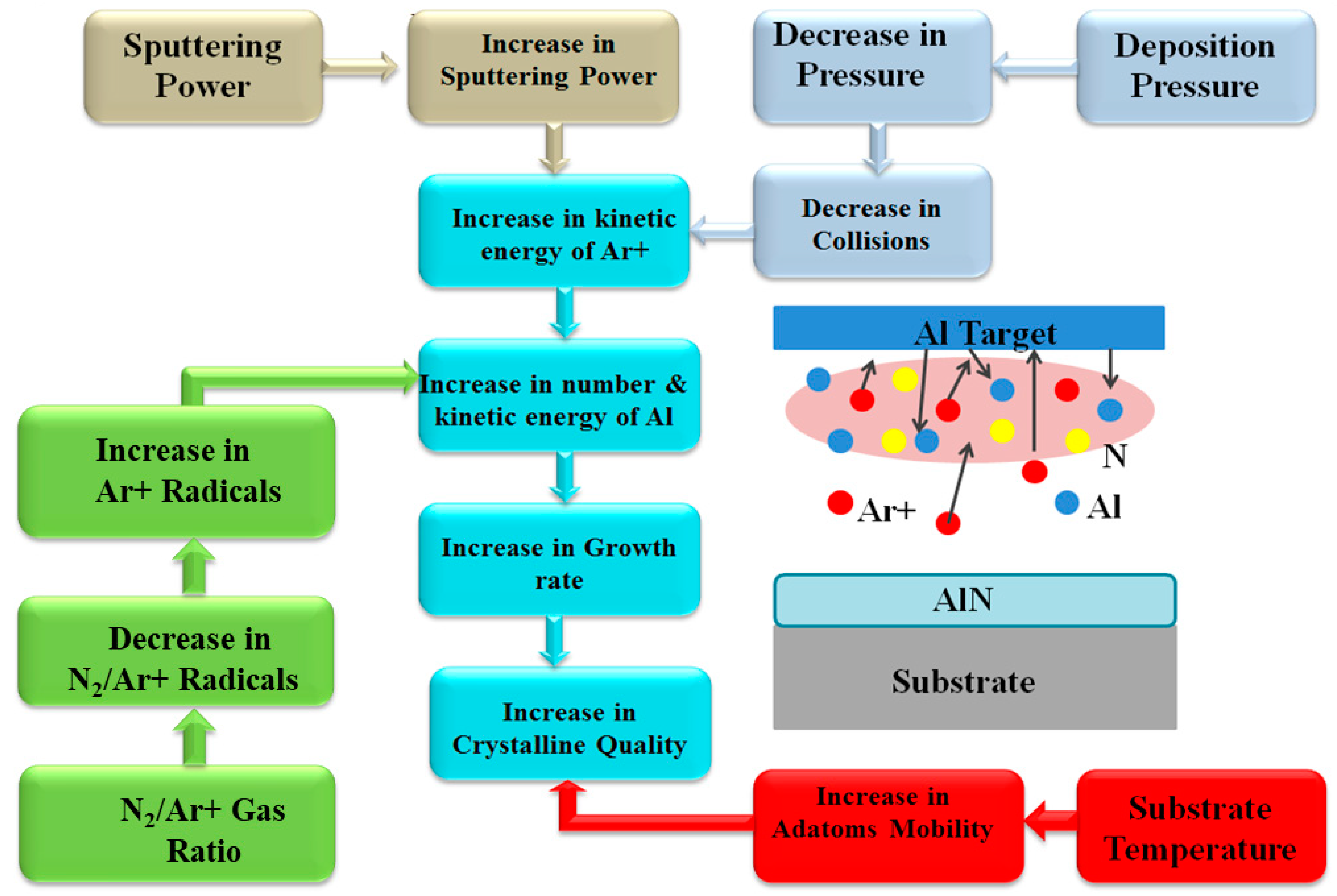
The data from Table 2 compiles the values of the sputtering parameters that had been used towards depositing highly c-axis AlN films. The reason for this compilation is as follows. These recipes could serve as reference points for any new work on the deposition of AlN film. Readers should be able to find the closest matches from Table 2 in term of their substrates and sputtering equipment. After locating the recipe(s), they should read the remaining sub-sections after Table 2 to understand the influences of different parameters to the deposition of highly c-axis film. The generic flow chart in Figure 5 summarizes them graphically, as well as highlighting the critical interactions between those sputtering parameters. With those information, reader should be able to commence the sputtering process, and subsequently alter their recipes based on the quality of the films.
The remainder of this section explains the roles of the sputtering parameters towards depositing the c-axis AlN films. The parameters are the choice of substrates, sputtering pressure, the sputtering power, the ratio of N2/Ar, the sputtering temperature, the film thickness, the distance between target to substrate, the substrate bias voltage, the base pressure, and the magnetic configuration. For each parameter, selected works that investigate its effect will be mentioned. In addition to using the works that were already summarized in Table 2, i.e., references [17,18,19,20,21,22,23,24,25,26,27,28,29,30,31,32,33,34,35,36,37,38,39,40,41,42,43,44,45,46,47,48,49,50,51,52,53,54,55,56,57,58,59,60,61,62], we also highlight additional articles that are not included in that table i.e., references [63,64,65,66,67,68,69,70,71,72,73,74,75,76,77,78,79,80,81,82,83,84,85,86] to illustrate the effect of specific parameters.
Finally, we mention in Section 3 that AlN is a unique material in a sense that it has a high mechanical, thermal and chemical stability. Therefore, we will discuss a few works [87,88,89,90] in Section 5.11 that sputtered and characterized their AlN thin films for applications in difficult environments. This information will be helpful for the new research that would like to employ this material to make sensors/devices at those conditions.
5.1. Choice of Substrates
Numerous research groups have successfully deposited c-axis oriented AlN on a broad range of substrates such Si (100), Si (111), titanium, molybdenum, aluminium, c-sapphire, aluminium oxide, microcrystalline diamond, glass, silicon dioxide, copper, silicon carbide, and chromium, etc. Table 2 lists them as well as the sputtering parameters and the qualities of the sputtered AlN films. While Si remains the preferred choice, researchers opted for other materials chiefly to reduce the lattice mismatch and the coefficient of thermal expansion (CTE) between these substrates and the c-axis AlN film. For example, the authors of this review made our contributions by sputtering AlN film on top of Si substrates with cubic silicon carbide (3C-SiC) buffer layers [8,16].
This is such an important parameter, that the previous review paper on similar topic performed their own investigations on the successful deposition of c-axis AlN film using multiple substrates namely Si, quartz, AlO2, MgO, MgAl2O4, and diamond. Then, Iriarte et al. [6] compiled the empirical results from all samples to plot the trend of the rest of sputtering parameters towards depositing highly c-axis AlN film.
5.2. Sputtering Pressure
According to the kinetic theory of molecular gasses, the ions, as well as the neutral species inside the sputtering chamber, have higher kinetic energies at lower process pressure. When they condense and are transformed to the solid state (called adatoms), they land on the surface of the substrate. The high kinetic energies create adatoms with faster mobility, which promote the high growth of c-axis AlN films [63]. It was also reported that when the sputtering pressure increased, the collision between sputtering particles and Ar ions led to the formation of AlN (100) films [64]. Both observations have been reported by many researchers in Table 2 such as in references [17,22,28,35,39,41,45].
One such works worth being mentioned in details herein. Cherng et al. [45] utilized a two-step deposition process to enhance the quality of deposited AlN on Si (100) using pulsed DC reactive sputtering. They used a smaller pressure of 0.8 mTorr for the initial nucleation for a period of 10 min. Afterwards, a second step was done at 2, 3.3, and 4.6 mTorr respectively. They observed that the two-steps sputtering resulted in smaller FWHM of the rocking curve as well as the smaller magnitude of residual stress. The value of the latter decreased from −926 to −317 MPa at a constant deposition rate of 36 nm/min.
Another group figured out the exact sputtering pressure before the AlN film orientation switched from the (002) to (100) planes. Kar et al. [65] investigated the effect of sputtering pressure on the crystal orientation and the morphological properties of deposited AlN on top of a p-type Si substrate. They observed the improved crystal quality for the AlN (002) film from 1.5 to 4.5 mTorr. After 6 mTorr, the crystal orientation changed to the (100) plane. They also observed that the surface roughness increased from 1.56 nm to 3.24 nm with the increasing pressure. In addition, the grain size was 114 nm until 4.5 mTorr pressure, and then decreased to 80 nm at 6 mTorr. The same switching trend was observed by another group. Taurino et al. [42] switched the AlN film orientation from the (002) to the (101) plane by increasing the pressure from 3 to 18 mTorr.
This observation seems to be valid on a variety of substrate materials. Singh et al. [39] employed Glass, Si, oxidized Si, Al–SiO2–Si, Cr– SiO2–Si, and Au–Cr–SiO2–Si substrates. They varied the sputtering pressure from 5, 10, and 20 mTorr and concluded that low pressure was favorable for the highly crystalline c-axis oriented AlN.
5.3. Sputtering Power
From experimental point of view, this is the easiest parameter to manipulate. Therefore, many research groups from Table 2 investigated the effect of this parameters towards producing highly c-axis AlN film [20,22,27,39,41,43,45,48,54,61]. A higher sputtering power means higher kinetic energies being supplied to the ions. In combination with the effect of sputtering pressure as explained in sub-section (5.2), many researchers employed high deposition power at low deposition pressure to get the best crystal-quality film. The power ranges from 100 W to 5.5 KW. However, several groups demonstrated that the high power can negatively affect the crystal quality of the AlN film because of an increase in the kinetic energies of the so-called secondary atoms.
A sputtering power in the range of 300 W to 500 W is typically used in RF sputtering, while a power in the range of 1000 W to 1800 W is typically employed in D.C. sputtering. The sputtering power also depends on the substrate to target distance and the type of sputtering system. For the former, a lower power is needed for a shorter distance.
In addition to the relationship between the sputtering power and crystal quality, Guo et al. [54] investigated the effect of RF power on the deposition rate, surface roughness, and optical transmittance. The last parameter refers to the fraction of incident light that passes via the AlN films. They observed that the deposition rate and the surface roughness increased and decreased, respectively, with the increase in RF power. The film exhibited around 75% optical transmission in the visible and ultraviolet ranges. From this optical data, they theorized that the increased RF power introduced defects in their film.
Another group documented the effect of the sputtering power on the grain size and residual stress of the film. Kusaka et al. [66] employed D.C. magnetron sputtering to deposit AlN films on a glass substrate at various sputtering powers. They observed that the grain size and the crystal quality improved with increasing power. Further, they noted that tensile stresses were obtained at lower power, while large compressive stresses were achieved at higher power.
Kumada et al. [67] documented the combined effect of sputtering power and N2 concentration in their studies. The former was varied from 200 to 900 W, and the latter from 30% to 70%. They produced AlN (101) and (002) poly crystals between 200–600 W at 50% N2 concentration, and AlN (002) film starting from 700 W power.
Finally, it should be mentioned that a two-steps deposition technique was also employed by few researchers. Lin et al. [68] tried to obtain a highly c-axis oriented AlN thin film on top of 3C-SiC/Si (100) substrate. First, they deposited a 50 nm nucleation layer at pure nitrogen using an AC power of 3 kW. Then, they ramped up the power to 5.5 kW. They obtained AlN (002) film with the lowest FWHM of rocking curve values of 1.73°.
5.4. N2 to Ar Ratio
Before covering the previous works that varied this parameter, we would like to explain the basic reactive sputtering. It has three modes, which is determined by the N2/Ar ratio. At lower N2 concentration i.e., “metal mode”, Al target is marginally covered with nitride. It is characterized by high deposition rate and high cathode voltage. Once N2 concentration increases, the “transition mode” occurs. The target surface becomes partially reactive with N2, resulting in a slight decrease in the deposition rate. The cathode voltage starts to decrease steeply because the higher secondary electron emission of the nitride being formed at the cathode surface pulled down the plasma impedance. Finally, the “Poison mode” is achieved when the entire target surface is covered with AlN compound. The cathode voltage and deposition rate are at their minimum level, and remains constant even at increasing N2 concentration. One of our published articles characterized this trend clearly in terms of discharged voltage and current. Readers are referred to Figure 1 from reference [8].
Table 2 listed the N2 to Ar ratio for all listed works. Some groups used lower and some groups used higher N2 concentrations to deposit highly c-axis AlN film. The past review paper by Iriarte et al. [6] had the same observation. In general, there are two opposite theories to explain the need for higher or lower N2/Ar ratio to grow AlN (002) film. While both agree that the kinetic energies of the smaller-mass N2 particles and bigger-mass Ar particles played major role in transferring the adatoms to the surface of the substrate, they differed on the end results. The groups who propagated the use of lower N2 concentrations argued that the AlN atomic bondings, i.e., B1 and B2, could only be created when Ar particles with the higher kinetic energies dominate. The group who needed the pure N2 concentration argued that the closed-pack (002) plane could only be assembled with lower surface energies, where N2 particles dominate. The details of both theories and their implications could be read in reference [69]. It should be noted that this is our own paper.
In this review paper, both factions are treated equally. First, we highlight the works from the groups that needed a lower N2/Ar ratio. Liu et al. [70] studied the effect of N2 concentrations in the range of 20% to 80%. They reported an FWHM of rocking curve value of 3.1° at 20% N2/Ar ratio. The value increase dramatically to 7.41° at 80% ratio. Zhong et al. [71] also reported the strong influence of the N2 concentration on the AlN films. They reported a decrease in the FWHM of the (002) diffraction peak amplitude when the N2 concentration increased from 25 to 75%. That effect is prominently displayed in Figure 1 of their article, Clement et al. [72] concurred and also observed the decreasing deposition rate at increasing N2 concentration.
We would also highlight the groups that could only achieved the c-axis AlN film at higher N2 concentration. Kar et al. [52] and Cheng et al. [64] specifically studied the effect of N2 concentrations on AlN film on top of Si (100) substrates. Both reported that at low N2 concentration, a strong (100) peak was observed. The increase in nitrogen concentration enhanced the (002) orientation. At pure N2, the films are fully (002) oriented.
The final point is as follows. Our group varied the N2 concentrations and observed different results for two substrates. The 3C-SiC-on-Si (100) and 3C-SiC-on-Si (111) have 28.6% and 1% lattice mismatches with AlN, respectively. The former requires a lower N2 concentration of about 40% [8]. The latter produced consistent (002) film at all N2 concentration [69]. Our hypothesis is that the smaller lattice mismatch plays a significant role in invalidating the effect of N2 concentrations.
5.5. Substrate Temperature
Substrate temperature largely influences the kinetic energy available to the adatoms on the surface of the deposited films. This energy increases proportionally with temperature, which helps in depositing the highly c-axis oriented films. However, after the optimal point, a further increase in the substrate temperature increases the thermal stresses in the film because of the CTE difference when the film is cooled down to room temperature. In addition, there are many impurities that are absorbed through the surface of the film at high temperature. Both factors decrease the film’s crystal quality [73]. Table 2 shows the ranges of the substrate temperature. It starts from the room temperature and could go up to 1000 °C [74].
The effect of substrate temperature on AlN orientation has been reported by numerous groups. A few are highlighted herein. Yang et al. [25] deposited AlN on top of Molybdenum (Mo). They carried out the sputtering at the following substrate temperatures: 20, 200, 400, and 600 °C. As the deposition temperature increased from 20 to 400 °C, the crystal orientation changed from (101) to (002). When the temperature was further increased to 600 °C, the intensity of the AlN (0002) peak decreased. Their results point to the existence of optimum temperature ranges for AlN (002) film. This was supported by another group. Jin et al. [31] deposited AlN film on top of Si (100) substrate. They used substrate temperatures of 60, 160, 250, 340, 430, and 520 °C. The deposition rate increased from 60 °C to 250 °C and saturated afterwards at 21.78 nm/min. The XRD results showed that the highest peak of the (002) orientation was observed at 430 °C. The intensity of the AlN (002) peak decreased afterwards. Our own work found similar optimum temperature range between 350 to 400 °C [73]. We deposited AlN film on top of 3C-SiC-0n-Si (111) substrate.
Medjani et al. [55] investigated the combined effects of substrate temperature and substrate bias. They RF sputtered AlN films on top of Si (100) substrate by varying the temperature from 25 to 800 °C and bias voltage from 0 to −100 V. It was found that the lower substrate temperature and moderate bias voltage helps in the formation of the (002) plane. A bias voltage smaller than −75 V and a temperature of 400 °C resulted in the growth of the (100) plane. Another group studied the effect of substrate temperature and N2 concentration on the surface roughness of the AlN film. Guo et al. [75] observed that the roughness increased linearly with substrate temperature and N2 concentrations.
There were not many works who performed the post annealing treatment on their sputtered films. Kar et al. [59] RF sputtered AlN film on top of Si substrate at 200 °C. After the samples cooled down, they subjected them to the annealing in N2 ambient for 90 s. The annealing temperature was increased from 400 to 1000 °C in steps of 200 °C. They observed that the intensity of AlN (002) diffraction peak increased until 800 °C, and then marginally decreased at 1000 °C. They also reported a small shift in the XRD diffraction peaks at higher annealing temperatures due to the residual stress. Also, the surface roughness (in rms) increased from 2.1 to 3.68 nm at annealing temperature of 400 to 1000 °C, respectively. Similar trend was found by Phan and Chung [34]. They annealed their samples for 1 h under N2 ambient at atmospheric pressure. They claimed superior performances of their Surface Acoustic Waves (SAW) devices after annealing.
5.6. Film Thickness
This is a very interesting parameter. It is a general knowledge that the thicker the film, the less sensitive it is to the lattice mismatch between the AlN and its substrate. The most prominent work on this parameter is perhaps from Iriarte et al. [6], who systematically studied the effect of AlN film thickness on a wide variety of substrates. Figure 5 of their paper shows the trend. The crystal quality increased with increasing thickness. After 1 μm film thickness however, the FWHM of the rocking curve values of the deposited films remained stagnant.
Other groups agree with that observation. Molleja et al. [26] investigated the role of AlN film thickness on its crystal quality and residual stress. The FWHM of the (002) diffraction peak decreased from 0.8 to 0.19 when the thickness was increased from 80 nm to 1.5 μm. They further reported that the thinner film had compressive stresses, while the thicker ones had tensile stress. Madrid et al. [30] supported Molleja’s group result by using the FWHM of the rocking curve measurement.
Other groups extended this observation to the piezoelectric properties of their films. Ababneh et al. [41] studied the effect of film thickness on the values of the d33 and d31 piezoelectric coefficients. They noticed that by increasing the AlN film thickness from 600 nm to 2,400 nm, the values for the d33 and d31 increases from 3.0 and −1.0 to 5.0 and −1.8 pm/V, respectively. Martin et al. [76] supported this trend. They deposited AlN films on top of Pt electrode with two different thicknesses i.e., 35 nm and 2 µm. They reported the FWHM of the rocking curve decreased from 2.60 to 1.14° and the value of the d33 increased from 2.75 to 5.15 pm/V. It is worth noting that the same group wrote the highly cited article that measure the piezoelectric coefficient of AlN [77], and on the regrowth of AlN film [78].
5.7. Target to Substrate Distance
The target to substrate distance could play a role in obtaining the c-axis AlN film. The exact degree of its significance has not been properly investigated. Most researchers agree that in the case of a smaller distance between the substrate and the target, the Al and N ions land on the substrate with higher kinetic energies and adatom mobilities due to the fewer collisions with other particles. On the other hand, when the distance is larger, these ions have multiple collisions with other particles before reaching the substrate. Thus, their kinetic energies and the subsequent adatoms mobilities decrease. From Table 2, target to substrate distances from 5 to 25 cm were used. The smaller distance is normally used for systems with higher powers. We further observed that most groups used the target to substrate distance from 3 to 8 cm for the sputtering power of 300 to 1000 W.
We highlight several groups who investigated the influence of the distance, in combination with other sputtering parameters. Xu et al. [79] deposited AlN film on Si (111) substrates using DC sputtering. They studied the effects of the sputtering pressure, sputtering power, and target to the substrate distance on the crystal orientation of the AlN films. The distance between the substrate to target was varied from 3 to 12 cm. They reported that a low sputtering pressure and shorter distance helped to form the (002) plane. On the contrary, a higher sputtering pressure and longer distance are beneficial for the growth of the (100) plane. The findings from this group was supported by Chen et al. [80], as well as Cheng et al. [63].
5.8. Substrate Bias Voltage
In some sputtering experiments, the substrates were biased with an RF source to attract the Al+ ions towards them. Table 2 listed these works [19,27,55,62]. It is generally known that the amplitude of the bias voltage corresponds to the landing kinetic energies of these ions, which in turn determine the crystal orientation. The substrate bias could also be used to increase the deposition rate and to tune the residual stress of the AlN film.
The formation of AlN (002) film requires higher biasing voltage when the low substrate temperature is used. Chu et al. [81] RF sputtered AlN thin films on top of glass substrates at room temperature. They applied different negative bias voltage from 0 to −320 V. The XRD diffraction showed a (002) oriented AlN up to −210 V. Afterwards, small diffraction peaks of AlN (002) and (100) planes were observed at a bias voltage of −240 V. Furthermore, the (002) plane vanished at the bias voltage of −320 V. The opposite trend is observed when the higher substrate temperature is used. One group reported a much lower amplitude to bias their substrate at the temperature of 200 °C. Iborra et al. [82] only needed a bias voltage of −24 V to achieve purely (002) oriented films. Finally, it is worth mentioning that Abdallah et al. [83] discusses the effect of compressive stress and ion bombardment on the orientation of the AlN film.
5.9. Base Pressure
Al has high affinity for oxygen (O2), and the combination of both elements degrades the crystalline quality of the AlN (002) film [6]. Therefore, the chamber is kept in an almost-vacuum condition to minimize O2. This is accomplished by constantly pumping out the gas/vapor without pumping in the Ar or N2 gasses, a method that is commonly known as outgassing. Table 2 listed the values of the base pressure that were used by many researchers. The range is between 3.6 × 10⁻³ to 3.6 × 10⁻⁷ Torr for the successful deposition of AlN film.
Cherng et al. [47] specifically studied the effect of outgassing on the deposition of AlN using pulsed-DC reactive sputtering of highly (002) oriented AlN thin film. They pumped down the system into the base pressure of 3 × 10⁻⁶ Torr, 1 × 10⁻⁶ Torr and 4 × 10⁻⁷ Torr before admitting the gas mixture into the chamber. They observed that both the FWHM of the rocking curve values and the residual stress became insensitive to the changes in the substrate temperature and deposition pressure at a lower base pressure. This was attributed to the less O2 contamination in the chamber.
5.10. Unbalanced Magnetron Configuration
Most published articles employ the conventional (balanced) magnetron configuration. In 1996, Window and Savvides [84] introduced the unbalanced configuration for sputtering system. It is able to increase the ion bombardments towards the substrate, at the price of rising substrate temperature. There are several groups who employed this technique for the deposition of AlN film. We highlight two of them in this review. Duquenne et al. [85] grew the film on top of Si (100) substrates with balanced and unbalanced configurations. By holding other parameters constant, the balanced system produced poly-crystal AlN with (100), (101) and (002) configurations. The unbalanced system produced only (002) plane, regardless of the N2 concentrations. This is attributed to the higher ion energy between 20–30 eV that is produced by that system. Another group compare the structural, morphological, and electric properties of AlN film that was grown on glass substrates in balanced and unbalanced configurations. Ke et al. [86] found that the latter configuration improves the AlN growth along the c-axis. The grains are denser and larger, and the film has smaller surface roughness, larger dielectric constant, and smaller leakage current.
5.11. Sputtered AlN (002) films for difficult environments
We discussed piezoelectric energy harvesters in Section 1. They could be very useful to power up electronics systems for difficult environments where conventional supplies are not practical, and the amplitude of the vibrations generate sufficient energies. Difficult environments include extreme temperatures and pressures, high mechanical shock and highly corrosive mediums. AlN is a good material candidate due to its higher mechanical, thermal, and chemical stability i.e., corrosion resistance.
There are many articles that characterized sputtered AlN’s mechanical and corrosion properties. Few examples are provided herein. Jian and Juang [87] employed nano-indentation technique to find out the hardness and deformation behavior of their sputtered c-axis film on sapphire substrate. They measured the value of film’s hardness and Young’s modulus as 16.2 and 243.5 GPa, respectively. Another group used AlN film as a protection material. Subramanian et al. [88] sputtered their AlN film as a coating material for mild steel (MS). That resulted in better wear resistance and a lower friction coefficient. We close this review paper by mentioning the newest applications of AlN film in life sciences. Reader is referred to a focus review on this topic in reference [89]. Towards that goal, one group RF sputtered AlN film and characterized its performance as biosensors, include its corrosion rate under saline solutions and compatibility with biological cells [90].
6. Conclusions
We analyzed around 80 journal articles that performed the reactive sputtering of c-axis AlN film on a wide variety of substrates and equipment. The data from Table 2 compiles the values of the sputtering parameters. These recipes could serve as reference points for any new work on the deposition of AlN film. Readers should be able to find the closest matches from Table 2 in term of their substrates and sputtering processes. In addition, the roles and ranges of the sputtering parameters in depositing c-axis oriented AlN film have been discussed.
The flow chart in Figure 5 illustrates the roles of major sputtering parameters in depositing c-axis AlN film. This chart is self-explanatory, but two points should be highlighted. The values of the landing kinetic energies of the ions and the surface mobility of the adatoms determine the specific crystal orientations of the film. We would like the adatoms to arrange themselves in the (002) plane. In order to achieve that, we need to adjust the values of all sputtering parameters to achieve the right balance. The number of runs to get the best quality films should be reduced if readers study Section 5.1, Section 5.2, Section 5.3, Section 5.4, Section 5.5, Section 5.6, Section 5.7, Section 5.8, Section 5.9 and Section 5.10 well.
Author Contributions
Conceptualization, A.I. and F.M.-Y.; Methodology, A.I. and F.M.-Y.; Formal Analysis, A.I. and F.M.-Y.; Data Curation, A.I. and F.M.-Y.; Writing-Original Draft Preparation, A.I.; Writing-Review & Editing, F.M.-Y.; Supervision, F.M.-Y.
Funding
This research received no external funding.
Acknowledgments
We would like express our gratitude to Alan Iacopi, Leonie Hold, Glenn Walker and Kien Chaik of Queensland Micro- and Nanotechnology Centre, and Alanna Fernandes of BluGlass Limited for their contributions to this PhD project. This work was performed in part at the Queensland node of the Australian National Fabrication Facility. A company established under the National Collaborative Research Infrastructure Strategy to provide nano and microfabrication facilities for Australia’s researchers. We also acknowledge Griffith School of Engineering for providing the PhD scholarships and financial supports for Abid Iqbal.
Conflicts of Interest
The authors declare no conflict of interest.
References
- Roundy, S.; Wright, P.K.; Rabaey, J.M. Energy Scavenging for Wireless Sensor Networks; Springer: Berlin, Germany, 2003. [Google Scholar]
- Dutoit, N.E.; Wardle, B.L.; Kim, S.-G. Design considerations for mems-scale piezoelectric mechanical vibration energy harvesters. Integr. Ferroelectr. 2005, 71, 121–160. [Google Scholar]
- Cook-Chennault, K.; Thambi, N.; Sastry, A. Powering mems portable devices—A review of non-regenerative and regenerative power supply systems with special emphasis on piezoelectric energy harvesting systems. Smart Mater. Struct. 2008, 17, 043001. [Google Scholar]
- Isarakorn, D.; Sambri, A.; Janphuang, P.; Briand, D.; Gariglio, S.; Triscone, J.; Guy, F.; Reiner, J.; Ahn, C.; de Rooij, N. Epitaxial piezoelectric mems on silicon. J. Micromech. Microeng. 2010, 20, 055008. [Google Scholar] [CrossRef]
- Kim, H.; Priya, S.; Stephanou, H.; Uchino, K. Consideration of impedance matching techniques for efficient piezoelectric energy harvesting. IEEE Trans. Ultrason. Ferroelectr. Freq. Control 2007, 54, 1851–1859. [Google Scholar] [CrossRef] [PubMed]
- Iriarte, G.; Rodriguez, J.; Calle, F. Synthesis of c-axis oriented AlN thin films on different substrates: A review. Mater. Res. Bull. 2010, 45, 1039–1045. [Google Scholar] [CrossRef]
- Iborra, E.; Olivares, J.; Clement, M.; Vergara, L.; Sanz-Hervás, A.; Sangrador, J. Piezoelectric properties and residual stress of sputtered AlN thin films for mems applications. Sens. Actuators A Phys. 2004, 115, 501–507. [Google Scholar]
- Iqbal, A.; Walker, G.; Iacopi, A.; Mohd-Yasin, F. Controlled sputtering of AlN (002) and (101) crystal orientations on epitaxial 3C-SiC-on-Si (100) substrate. J. Cryst. Growth 2016, 440, 76–80. [Google Scholar]
- Elfrink, R.; Kamel, T.; Goedbloed, M.; Matova, S.; Hohlfeld, D.; Van Andel, Y.; Van Schaijk, R. Vibration energy harvesting with aluminum nitride-based piezoelectric devices. J. Micromech. Microeng. 2009, 19, 094005. [Google Scholar] [CrossRef]
- Boeshore, S.E. Aluminum Nitride Thin Films on Titanium: Piezoelectric Transduction on a Metal Substrate; ProQuest: Ann Arbor, MI, USA, 2006. [Google Scholar]
- Ruiz, E.; Alvarez, S.; Alemany, P. Electronic structure and properties of ALN. Phys. Rev. B 1994, 49, 7115. [Google Scholar] [CrossRef]
- Cimalla, V.; Pezoldt, J.; Ambacher, O. Group III nitride and sic based mems and nems: Materials properties, technology and applications. J. Phys. D Appl. Phys. 2007, 40, 6386. [Google Scholar]
- Levinshtein, M.E.; Shur, M.S.; Rumyantsev, S.L.; Shur, M.S. Properties of Advanced Semiconductor Materials: GaN, AIN, InN, BN, SiC, SiGe; John Wiley & Sons: Hoboken, NJ, USA, 2001. [Google Scholar]
- Edgar, J.H. Properties of Group III Nitrides; Institution of Electrical Engineers: London, UK, 1994. [Google Scholar]
- Suetsugu, T.; Yamazaki, T.; Tomabechi, S.; Wada, K.; Masu, K.; Tsubouchi, K. ALN epitaxial growth on atomically flat initially nitrided α-Al2O3 wafer. Appl. Surf. Sci. 1997, 117, 540–545. [Google Scholar] [CrossRef]
- Iqbal, A.; Chaik, K.; Walker, G.; Iacopi, A.; Mohd-Yasin, F.; Dimitrijev, S. RF sputtering of polycrystalline (100), (002), and (101) oriented AlN on an epitaxial 3C-SIC (100) on Si (100) substrate. J. Vac. Sci. Technol. B 2014, 32, 06F401. [Google Scholar] [CrossRef]
- Ohtsuka, M.; Takeuchi, H.; Fukuyama, H. Effect of sputtering pressure on crystalline quality and residual stress of AlN films deposited at 823 K on nitrided sapphire substrates by pulsed dc reactive sputtering. Jpn. J. Appl. Phys. 2016, 55, 05FD08. [Google Scholar] [CrossRef]
- Stan, G.; Botea, M.; Boni, G.; Pintilie, I.; Pintilie, L. Electric and pyroelectric properties of AlN thin films deposited by reactive magnetron sputtering on Si substrate. Appl. Surface Sci. 2015, 353, 1195–1202. [Google Scholar] [CrossRef]
- Wang, J.; Zhang, Q.; Yang, G.; Yao, C.; Li, Y.; Sun, R.; Zhao, J.; Gao, S. Effect of substrate temperature and bias voltage on the properties in dc magnetron sputtered AlN films on glass substrates. J. Mater. Sci. Mater. Electron. 2016, 27, 3026–3032. [Google Scholar] [CrossRef]
- Jiao, X.; Shi, Y.; Zhong, H.; Zhang, R.; Yang, J. ALN thin films deposited on different Si-based substrates through RF magnetron sputtering. J. Mater. Sci. Mater. Electron. 2015, 26, 801–808. [Google Scholar] [CrossRef]
- Bi, X.; Wu, Y.; Wu, J.; Li, H.; Zhou, L. A model for longitudinal piezoelectric coefficient measurement of the aluminum nitride thin films. J. Mater. Sci. Mater. Electron. 2014, 25, 2435–2442. [Google Scholar] [CrossRef]
- Shih, W.-C.; Chen, Y.-C.; Chang, W.-T.; Cheng, C.-C.; Liao, P.-C.; Kao, K.-S. Design and fabrication of nanoscale IDTs using electron beam technology for high-frequency saw devices. J. Nanomater. 2014, 2014, 643672. [Google Scholar] [CrossRef]
- Stoeckel, C.; Kaufmann, C.; Hahn, R.; Schulze, R.; Billep, D.; Gessner, T. Pulsed dc magnetron sputtered piezoelectric thin film aluminum nitride–technology and piezoelectric properties. J. Appl. Phys. 2014, 116, 034102. [Google Scholar] [CrossRef]
- Lim, W.T.; Son, B.K.; Kang, D.H.; Lee, C.H. Structural properties of AlN films grown on Si, Ru/Si and ZnO/Si substrates. Thin Solid Films 2001, 382, 56–60. [Google Scholar] [CrossRef]
- Yang, J.; Jiao, X.; Zhang, R.; Zhong, H.; Shi, Y.; Du, B. Growth of AlN films as a function of temperature on Mo films deposited by different techniques. J. Electron. Mater. 2014, 43, 369–374. [Google Scholar] [CrossRef]
- García Molleja, J.; Gómez, B.J.; Ferrón, J.; Gautron, E.; Bürgi, J.; Abdallah, B.; Djouadi, M.A.; Feugeas, J.; Jouan, P.-Y. AlN thin films deposited by dc reactive magnetron sputtering: Effect of oxygen on film growth. Eur. Phys. J. Appl. Phys. 2013, 64, 20302. [Google Scholar] [CrossRef]
- Monteagudo-Lerma, L.; Valdueza-Felip, S.; Núñez-Cascajero, A.; González-Herráez, M.; Monroy, E.; Naranjo, F. Two-step method for the deposition of AlN by radio frequency sputtering. Thin Solid Films 2013, 545, 149–153. [Google Scholar] [CrossRef] [Green Version]
- Aissa, K.A.; Achour, A.; Camus, J.; Le Brizoual, L.; Jouan, P.-Y.; Djouadi, M.-A. Comparison of the structural properties and residual stress of AlN films deposited by dc magnetron sputtering and high power impulse magnetron sputtering at different working pressures. Thin Solid Films 2014, 550, 264–267. [Google Scholar] [CrossRef]
- Kale, A.; Brusa, R.; Miotello, A. Structural and electrical properties of AlN films deposited using reactive rf magnetron sputtering for solar concentrator application. Appl. Surf. Sci. 2012, 258, 3450–3454. [Google Scholar] [CrossRef]
- Rodríguez-Madrid, J.; Iriarte, G.; Araujo, D.; Villar, M.; Williams, O.A.; Müller-Sebert, W.; Calle, F. Optimization of AlN thin layers on diamond substrates for high frequency saw resonators. Mater. Lett. 2012, 66, 339–342. [Google Scholar] [CrossRef] [Green Version]
- Jin, H.; Feng, B.; Dong, S.; Zhou, C.; Zhou, J.; Yang, Y.; Ren, T.; Luo, J.; Wang, D. Influence of substrate temperature on structural properties and deposition rate of AlN thin film deposited by reactive magnetron sputtering. J. Electron. Mater. 2012, 41, 1948–1954. [Google Scholar] [CrossRef]
- Ababneh, A.; Alsumady, M.; Seidel, H.; Manzaneque, T.; Hernando-García, J.; Sánchez-Rojas, J.; Bittner, A.; Schmid, U. C-axis orientation and piezoelectric coefficients of AlN thin films sputter-deposited on titanium bottom electrodes. Appl. Surf. Sci. 2012, 259, 59–65. [Google Scholar] [CrossRef]
- García-Gancedo, L.; Zhu, Z.; Iborra, E.; Clement, M.; Olivares, J.; Flewitt, A.; Milne, W.; Ashley, G.; Luo, J.; Zhao, X. AlN-based Baw resonators with CNT electrodes for gravimetric biosensing. Sens. Actuators B Chem. 2011, 160, 1386–1393. [Google Scholar] [CrossRef] [Green Version]
- Phan, D.-T.; Chung, G.-S. The effect of geometry and post-annealing on surface acoustic wave characteristics of AlN thin films prepared by magnetron sputtering. Appl. Surf. Sci. 2011, 257, 8696–8701. [Google Scholar] [CrossRef]
- Singh, A.V.; Chandra, S.; Srivastava, A.; Chakroborty, B.; Sehgal, G.; Dalai, M.; Bose, G. Structural and optical properties of RF magnetron sputtered aluminum nitride films without external substrate heating. Appl. Surf. Sci. 2011, 257, 9568–9573. [Google Scholar] [CrossRef]
- Cardenas-Valencia, A.M.; Onishi, S.; Rossie, B. Single-crystalline AlN growth on sapphire using physical vapor deposition. Phys. Lett. A 2011, 375, 1000–1004. [Google Scholar] [CrossRef]
- Iriarte, G.; Reyes, D.; González, D.; Rodriguez, J.; García, R.; Calle, F. Influence of substrate crystallography on the room temperature synthesis of AlN thin films by reactive sputtering. Appl. Surf. Sci. 2011, 257, 9306–9313. [Google Scholar] [CrossRef]
- Moreira, M.; Doi, I.; Souza, J.; Diniz, J. Electrical characterization and morphological properties of AlN films prepared by dc reactive magnetron sputtering. Microelectron. Eng. 2011, 88, 802–806. [Google Scholar] [CrossRef]
- Singh, A.V.; Chandra, S.; Bose, G. Deposition and characterization of c-axis oriented aluminum nitride films by radio frequency magnetron sputtering without external substrate heating. Thin Solid Films 2011, 519, 5846–5853. [Google Scholar] [CrossRef]
- Subramanian, B.; Swaminathan, V.; Jayachandran, M. Micro-structural and optical properties of reactive magnetron sputtered aluminum nitride (AlN) nanostructured films. Curr. Appl. Phys. 2011, 11, 43–49. [Google Scholar] [CrossRef]
- Ababneh, A.; Schmid, U.; Hernando, J.; Sánchez-Rojas, J.; Seidel, H. The influence of sputter deposition parameters on piezoelectric and mechanical properties of AlN thin films. Mater. Sci. Eng. B 2010, 172, 253–258. [Google Scholar] [CrossRef]
- Taurino, A.; Signore, M.; Catalano, M.; Kim, M. (101) and (002) oriented AlN thin film deposited by sputtering. Mater. Lett. 2017, 200. [Google Scholar] [CrossRef]
- Vashaei, Z.; Aikawa, T.; Ohtsuka, M.; Kobatake, H.; Fukuyama, H.; Ikeda, S.; Takada, K. Influence of sputtering parameters on the crystallinity and crystal orientation of AlN layers deposited by rf sputtering using the AlN target. J. Cryst. Growth 2009, 311, 459–462. [Google Scholar] [CrossRef]
- Clement, M.; Olivares, J.; Iborra, E.; González-Castilla, S.; Rimmer, N.; Rastogi, A. Aln films sputtered on iridium electrodes for bulk acoustic wave resonators. Thin Solid Films 2009, 517, 4673–4678. [Google Scholar] [CrossRef]
- Cherng, J.; Lin, C.; Chen, T. Two-step reactive sputtering of piezoelectric AlN thin films. Surf. Coat. Technol. 2008, 202, 5684–5687. [Google Scholar] [CrossRef]
- Abdallah, B.; Duquenne, C.; Besland, M.; Gautron, E.; Jouan, P.; Tessier, P.; Brault, J.; Cordier, Y.; Djouadi, M. Thickness and substrate effects on AlN thin film growth at room temperature. Eur. Phys. J. Appl. Phys. 2008, 43, 309–313. [Google Scholar] [CrossRef]
- Cherng, J.; Chang, D. Effects of outgassing on the reactive sputtering of piezoelectric AlN thin films. Thin Solid Films 2008, 516, 5292–5295. [Google Scholar] [CrossRef]
- Chiu, K.-H.; Chen, J.-H.; Chen, H.-R.; Huang, R.-S. Deposition and characterization of reactive magnetron sputtered aluminum nitride thin films for film bulk acoustic wave resonator. Thin Solid Films 2007, 515, 4819–4825. [Google Scholar] [CrossRef]
- Kano, K.; Arakawa, K.; Takeuchi, Y.; Akiyama, M.; Ueno, N.; Kawahara, N. Temperature dependence of piezoelectric properties of sputtered AlN on silicon substrate. Sens. Actuators A Phys. 2006, 130, 397–402. [Google Scholar] [CrossRef]
- Venkataraj, S.; Severin, D.; Drese, R.; Koerfer, F.; Wuttig, M. Structural, optical and mechanical properties of aluminium nitride films prepared by reactive dc magnetron sputtering. Thin Solid Films 2006, 502, 235–239. [Google Scholar] [CrossRef]
- Benetti, M.; Cannata, D.; Di Pietrantonio, F.; Verona, E.; Generosi, A.; Paci, B.; Albertini, V.R. Growth and characterization of piezoelectric AlN thin films for diamond-based surface acoustic wave devices. Thin Solid Films 2006, 497, 304–308. [Google Scholar] [CrossRef]
- Kar, J.; Bose, G.; Tuli, S. Influence of nitrogen concentration on grain growth, structural and electrical properties of sputtered aluminum nitride films. Scr. Mater. 2006, 54, 1755–1759. [Google Scholar] [CrossRef]
- Umeda, K.; Takeuchi, M.; Yamada, H.; Kubo, R.; Yoshino, Y. Improvement of thickness uniformity and crystallinity of AlN films prepared by off-axis sputtering. Vacuum 2006, 80, 658–661. [Google Scholar] [CrossRef]
- Guo, Q.; Tanaka, T.; Nishio, M.; Ogawa, H. Growth properties of AlN films on sapphire substrates by reactive sputtering. Vacuum 2006, 80, 716–718. [Google Scholar] [CrossRef]
- Medjani, F.; Sanjines, R.; Allidi, G.; Karimi, A. Effect of substrate temperature and bias voltage on the crystallite orientation in rf magnetron sputtered AlN thin films. Thin Solid Films 2006, 515, 260–265. [Google Scholar] [CrossRef]
- Vergara, L.; Olivares, J.; Iborra, E.; Clement, M.; Sanz-Hervás, A.; Sangrador, J. Effect of rapid thermal annealing on the crystal quality and the piezoelectric response of polycrystalline AlN films. Thin Solid Films 2006, 515, 1814–1818. [Google Scholar] [CrossRef]
- Kar, J.; Bose, G.; Tuli, S. Correlation of electrical and morphological properties of sputtered aluminum nitride films with deposition temperature. Curr. Appl. Phys. 2006, 6, 873–876. [Google Scholar] [CrossRef]
- Jang, K.; Lee, K.; Kim, J.; Hwang, S.; Lee, J.; Dhungel, S.K.; Jung, S.; Yi, J. Effect of rapid thermal annealing of sputtered aluminium nitride film in an oxygen ambient. Mater. Sci. Semicond. Process. 2006, 9, 1137–1141. [Google Scholar] [CrossRef]
- Kar, J.; Bose, G.; Tuli, S. Influence of rapid thermal annealing on morphological and electrical properties of rf sputtered AlN films. Mater. Sci. Semicond. Process. 2005, 8, 646–651. [Google Scholar] [CrossRef]
- Iriarte, G.F.; Bjurstrom, J.; Westlinder, J.; Engelmark, F.; Katardjiev, I.V. Synthesis of c-axis-oriented AlN thin films on high-conducting layers: Al, Mo, Ti, Tin, and Ni. IEEE Trans. Ultrason. Ferroelectr. Freq. Control 2005, 52, 1170–1174. [Google Scholar] [CrossRef] [PubMed]
- Zhang, J.; Cheng, H.; Chen, Y.; Uddin, A.; Yuan, S.; Geng, S.; Zhang, S. Growth of AlN films on Si (100) and Si (111) substrates by reactive magnetron sputtering. Surf. Coat. Technol. 2005, 198, 68–73. [Google Scholar] [CrossRef]
- Sanz-Hervas, A.; Vergara, L.; Olivares, J.; Iborra, E.; Morilla, Y.; Garcia-Lopez, J.; Clement, M.; Sangrador, J.; Respaldiza, M. Comparative study of c-axis AlN films sputtered on metallic surfaces. Diam. Relat. Mater. 2005, 14, 1198–1202. [Google Scholar] [CrossRef]
- Cheng, H.E.; Lin, T.C.; Chen, W.C. Preparation of [002] oriented AlN thin films by mid frequency reactive sputtering technique. Thin Solid Films 2003, 425, 85–89. [Google Scholar] [CrossRef]
- Cheng, H.; Sun, Y.; Zhang, J.; Zhang, Y.; Yuan, S.; Hing, P. AlN films deposited under various nitrogen concentrations by RF reactive sputtering. J. Cryst. Growth 2003, 254, 46–54. [Google Scholar] [CrossRef]
- Kar, J.; Bose, G.; Tuli, S. A study on the interface and bulk charge density of AlN films with sputtering pressure. Vacuum 2006, 81, 494–498. [Google Scholar] [CrossRef]
- Kusaka, K.; Taniguchi, D.; Hanabusa, T.; Tominaga, K. Effect of input power on crystal orientation and residual stress in AlN film deposited by dc sputtering. Vacuum 2000, 59, 806–813. [Google Scholar] [CrossRef]
- Kumada, T.; Ohtsuka, M.; Takada, K.; Fukuyama, H. Influence of sputter power and n2 gas flow ratio on crystalline quality of AlN layers deposited at 823 k by rf reactive sputtering. Phys. Status Solidi 2012, 9, 515–518. [Google Scholar] [CrossRef]
- Lin, C.-M.; Lien, W.-C.; Yen, T.-T.; Felmetsger, V.V.; Senesky, D.G.; Hopcroft, M.A.; Pisano, A.P. Growth of highly c-axis oriented AlN films on 3C–SiC/Si substrate. In Proceedings of the Solid-State Sensors, Actuators, and Microsystems Workshop, Hilton Head Island, SC, USA, 6–10 June 2010; pp. 324–327. [Google Scholar]
- Iqbal, A.; Walker, G.; Hold, L.; Fernandes, A.; Iacopi, A.; Mohd-Yasin, F. DC sputtering of highly c-axis AlN films on top of 3C-SiC (111)-on-Si (111) substrate under various N2 concentrations. J. Vac. Sci. Technol. B 2017, 35, 06GH01. [Google Scholar] [CrossRef]
- Liu, H.; Tang, G.; Zeng, F.; Pan, F. Influence of sputtering parameters on structures and residual stress of AlN films deposited by DC reactive magnetron sputtering at room temperature. J. Cryst. Growth 2013, 363, 80–85. [Google Scholar] [CrossRef]
- Zhong, H.; Xiao, Z.; Jiao, X.; Yang, J.; Wang, H.; Zhang, R.; Shi, Y. Residual stress of AlN films RF sputter deposited on Si (111) substrate. J. Mater. Sci. Mater. Electron. 2012, 23, 2216–2220. [Google Scholar] [CrossRef]
- Clement, M.; Iborra, E.; Sangrador, J.; Sanz-Hervás, A.; Vergara, L.; Aguilar, M. Influence of sputtering mechanisms on the preferred orientation of aluminum nitride thin films. J. Appl. Phys. 2003, 94, 1495–1500. [Google Scholar] [CrossRef]
- Iqbal, A.; Walker, G.; Hold, L.; Fernandes, A.; Tanner, P.; Iacopi, A.; Mohd-Yasin, F. The sputtering of AlN films on top of on- and off-axis 3C-SiC (111)-on-Si (111) substrates at various substrate temperatures. J. Mater. Sci. Mater. Electron. 2018, 29, 2434–2446. [Google Scholar] [CrossRef]
- Tungamista, S.; Birch, J.; Persson, P.; Jarrendahl, K.; Hultman, L. Enhanced quality of epitaxial AlN thin films on 6H-SiC by ultra high vacuum ion assisted reactive dc magnetron sputter deposition. Appl. Phys. Lett. 2000, 76, 170–172. [Google Scholar]
- Guo, Q.; Yoshitugu, M.; Tanaka, T.; Nishio, M.; Ogawa, H. Microscopic investigations of aluminum nitride thin films grown by low-temperature reactive sputtering. Thin Solid Films 2005, 483, 16–20. [Google Scholar] [CrossRef]
- Martin, F.; Muralt, P.; Dubois, M.-A.; Pezous, A. Thickness dependence of the properties of highly c-axis textured AlN thin films. J. Vac. Sci. Technol. A 2004, 22, 361–365. [Google Scholar] [CrossRef]
- Dubois, M.A.; Muralt, P. Stress and piezoelectric properties of aluminum nitride thin film deposited on metal electrodes by pulsed direct current reactive sputtering. J. Appl. Phys. 2001, 89, 6389–6395. [Google Scholar] [CrossRef]
- Martin, F.; Muralt, P.; Cantoni, M.; Dubois, M.A. Re-growth of c-axis oriented AlN thin film. In Proceedings of the IEEE Ultrasonics Symposium, Montreal, QC, Canada, 23–27 August 2004. [Google Scholar]
- Xu, X.H.; Wu, H.S.; Zhang, C.J.; Jin, Z.H. Morphological properties of AlN piezoelectric thin films deposited by DC reactive magnetron sputtering. Thin Solid Films 2001, 388, 62–67. [Google Scholar] [CrossRef]
- Chen, Y.; Wang, R.; Wang, B.; Xing, T.; Song, X.; Zhu, M.; Yan, H. Effects of mean free path on the preferentially orientated growth of AlN thin films. J. Cryst. Growth 2005, 283, 315–319. [Google Scholar] [CrossRef]
- Chu, A.; Chao, C.; Lee, F.; Huang, H. Influences of bias voltage on the crystallographic orientation of AlN thin films prepared by long-distance magnetron sputtering. Thin Solid Films 2003, 429, 1–4. [Google Scholar] [CrossRef]
- Iborra, E.; Clement, M.; Sangrador, J.; Sanz-Hervás, A.; Vergara, L.; Aguilar, M. Effect of particle bombardment on the orientation and the residual stress of sputtered AlN films for SAW devices. IEEE Trans. Ultrason. Ferroelectr. Freq. Control 2004, 51, 352–358. [Google Scholar] [CrossRef] [PubMed]
- Abdallah, B.; Challa, A.; Jouan, P.Y.; Besland, M.P.; Djouadi, M.A. Deposition of AlN films by reactive sputtering: Effect of radio frequency substrate bias. Thin Solid Films 2007, 515, 7105–7108. [Google Scholar] [CrossRef]
- Window, B.; Savvides, N. Unbalanced dc magnetron as sources of high ion fluxes. J. Vac. Sci. Technol. A 1996, 4, 453–456. [Google Scholar] [CrossRef]
- Duquenne, C.; Tessier, P.Y.; Besland, M.P.; Angleroud, B.; Jouan, P.Y.; Aubry, R.; Delage, S.; Djouadi, M. Impact of magnetron configuration on plasma and film properties of sputtered aluminum nitride thin films. J. Appl. Phys. 2008, 104, 063301. [Google Scholar] [CrossRef]
- Ke, G.; Tao, Y.; Lu, Y.; Bian, Y.; Zhu, T.; Guo, H.; Chen, Y. Highly c-axis oriented AlN film grown by unbalanced magnetron reactive sputtering and its electrical properties. J. Alloys Compd. 2015, 646, 446–453. [Google Scholar] [CrossRef]
- Jian, S.-R.; Juang, J.-Y. Indentation-induced mechanical deformation behaviors of AlN thin films deposited on c-plane sapphire. J. Nanomater. 2012, 2012, 914184. [Google Scholar] [CrossRef]
- Subramanian, B.; Ashok, K.; Jayachandran, M. Structure, mechanical and corrosion properties of DC reactive magnetron sputtered aluminum nitride (AlN) hard coatings on mild steel substrates. J. Appl. Electrochem. 2008, 38, 619–625. [Google Scholar] [CrossRef]
- Fu, Y.Q.; Luo, J.K.; Nguyen, N.T.; Walton, A.J.; Flewitt, A.J.; Zu, X.T.; Li, Y.; McHale, G.; Matthews, A.; Iborrac, E.; et al. Advances in piezoelectric thin films for acoustic biosensors, acoustofluidics and lab-on-chip applications. Prog. Mater. Sci. 2017, 89, 31–91. [Google Scholar] [CrossRef]
- Besleaga, C.; Dumitru, V.; Trinca, L.M.; Popa, A.C.; Negrila, C.C.; Kołodziejczyk, Ł.; Luculescu, C.R.; Ionescu, G.C.; Ripeanu, R.G.; Vladescu, A.; et al. Mechanical, Corrosion and Biological Properties of Room-Temperature Sputtered Aluminum Nitride Films with Dissimilar Nanostructure. Nanomaterials 2017, 7, 394. [Google Scholar] [CrossRef] [PubMed]
Figure 1.
Piezoelectric transduction of mechanical to electrical energies.

Figure 2.
(a) Crystal structure; (b) B1 and B2 bonds; (c) crystal structure with B1 and B2 bonds; and (d) different planes of AlN.
Figure 2.
(a) Crystal structure; (b) B1 and B2 bonds; (c) crystal structure with B1 and B2 bonds; and (d) different planes of AlN.

Figure 3.
The example of XRD plot of AlN films [8]. There are four panels in the figure, denoting the crystal orientations of four films that were deposited with different Nitrogen concentrations. The AlN peaks are (100), (101), (102) and (002). The y-axis has an arbitrary unit.
Figure 3.
The example of XRD plot of AlN films [8]. There are four panels in the figure, denoting the crystal orientations of four films that were deposited with different Nitrogen concentrations. The AlN peaks are (100), (101), (102) and (002). The y-axis has an arbitrary unit.

Figure 4.
Reactive sputtering process for AlN film [16].
Figure 4.
Reactive sputtering process for AlN film [16].

Figure 5.
Flow chart on the role of sputtering parameters towards depositing c-axis AlN.


| Structural Properties | Density (g/cm3) | 3.257 |
| Elastic modulus (GPa) | 330 | |
| Elastic constant C11 (GPa) | 410 ± 10 | |
| Elastic constant C12 (GPa) | 149 ± 1 | |
| Elastic constant C13 (GPa) | 99 ± 4 | |
| Poisson’s ratio | 0.22 | |
| Crystal structure | Wurtzite | |
| Lattice constant (Å) | a = 3.112 c = 4.982 | |
| Hardness (Kg/mm2) | 1100 | |
| Water absorption | None | |
| Optical Properties | Density of states in conduction band (cm−3) | 4.1 × 10¹⁸ |
| Effective hole mass | mhz = 3.53 m0 mhx = 10.42 m0 | |
| Density of states in valence band (cm−3) | 4.8 × 10²⁰ | |
| Optical phonon energy (meV) | 113 | |
| Refractive index (visible to IR) | ~2.15 | |
| Electrical Properties | Breakdown field (V/cm) | 1.2–1.8 × 10⁶ |
| Mobility of electrons/holes (cm2/V·s) | 135/14 | |
| Dielectric constant (static/high frequency) | 8.5–9.14/4.6–4.84 | |
| Energy band gap (eV) | 6.13–6.23 | |
| Resistivity (Ohm·cm) | 1015 | |
| Thermal Properties | Thermal conductivity (W/m·°K) | 140–180 |
| Coefficient of thermal expansion (×10−6/°C) | 4.2–5.3 | |
| Debye temperature (°K) | 1150 | |
| Melting Point (°C) | 2200 | |
| Piezoelectric Properties | Piezoelectric coefficient e15 (C/m2) | −0.33~−0.48 |
| Piezoelectric coefficient e31 (C/m2) | −0.38~−0.82 | |
| Piezoelectric coefficient e33 (C/m2) | 1.26–2.1 | |
| Relative permittivity coefficient ɛ11 | 9 | |
| Relative permittivity coefficient ε22 | 9 | |
| Relative permittivity coefficient ε33 | 11 |
Table 2.
Summary of published works on the deposition of c-axis AlN films.
| Authors [ref] (Year of Publication) | Substrate | Sputtering Type | Power (W)/Power Density (W/cm2) | Substrate Temperature (°C) | Sputtering Pressure (mTorr) | Base Pressure (mbar) | Nitrogen (%) | Total Gas (sccm) | Distance Target to Substrate (cm) | FWHM (°) | Deposition Rate (nm/min) | Film Thickness (µm) | Surface Roughness (nm) | Notes |
|---|---|---|---|---|---|---|---|---|---|---|---|---|---|---|
| Ohtsuka et al. [17] (2016) | sapphire | Pulsed DC magnetron sputtering | 800/9.86 | 550 | 3 to 11 | - | 50 | - | 6 | 3.3 (rocking curve) | 60 | 1.5 | - | Effect of sputtering pressure on crystalline quality and residual stress. |
| Stan et al. [18] (2015) | Si | RF magnetron sputtering | - | 50 | 1.5 | - | 25 | 40 | 3.5 | 11, 7.1 (rocking curve) | 19 | 0.6, 1.1 | 0.5 to 1.6 | Investigated electric and pyroelectric properties of deposited films. |
| Wang et al. [19] (2016) | Glass | DC magnetron sputtering | 170/9.55 | 400 | 9 | - | 15 | 35 | 4.7 | - | 66.5 | 8.35 | 48 | Effects of substrate temperature and bias voltage on crystal orientation. |
| Jiao et al. [20] (2015) | Si (100), Si (111), SiO2, and amorphous Si (α-Si) | RF Magnetron sputtering | 150, 200, 250, 300/5.3, 7.07, 8.84, 10.6 | 25 | 5 | 5 × 10⁻⁴ | 50, 66, 75, 80 | 60 | 6 | - | - | - | 4.22 | Effect of various Si substrates on film quality. Effect of RF power and gas flow on residual stress and film quality. |
| Bi et al. [21] (2014) | Si (100) | DC magnetron sputtering | 460/5.34 | 400 | 3 | 1 × 10⁻¹⁰ | 85 | 22.8 | 7.5 | 1.63 (rocking curve) | 7.5 | 1.8 | - | Measured the longitudinal piezoelectric coefficient of deposited films. |
| Shih et al. [22] (2014) | Si3N4/Si | RF Magnetron sputtering | 200, 250, 300/NA | 300 | 5, 10, 15 | 6.6 × 10⁻⁸ | 60 | 5 | - | 11.2 | 1.9 | 6.42 | Effect of RF power and sputtering pressure on film quality. Fabricated SAW device. | |
| Stoeckel et al. [23] (2014) | Si (100) | Pulsed DC magnetron sputtering | 865/7.6 | 350 | 5.25 | - | 80 | 7.5 | 0.39 (diffraction peak) | 0.204 | - | - | Measured transverse piezoelectric coefficient d31 using laser Doppler vibrometer (LDV). | |
| Lim et al. [24] (2001) | Si, Ru/Si and ZnO/Si | RF magnetron sputtering | - | 150 | 0.5 | - | 50 | - | 5 | 5.96, 4.05, 1.19 (rocking curve) | 8.4 | 0.5 to 0.6 | - | Efects of Si, Ru/Si and ZnO/Si substrates on the crystal quality of AlN film. |
| Yang et al. [25] (2014) | Mo/Si (100) | RF magnetron sputtering | 200/7.07 | 20 to 600 | 7.5 | 2 × 10⁻⁷ | 50 | 6.5 | 2.4 (rocking curve) | - | - | - | Effect of substrate temperature on film quality. | |
| García Molleja et al. [26] (2013) | SiO2/Si (100) | DC reactive magnetron sputtering | 100/11.68 | 25 | 3 | 2 × 10⁻⁸ | 30 | 3 | 0.8 to 0.19 (diffraction peak) | - | 1.5 | - | Effect of film thickness on residual stress and film quality. | |
| Monteagudo-Lerma et al. [27] (2013) | C-sapphire | RF reactive sputtering | 100–175/5.1–8.94 | 400 | 3.5 | 1 × 10⁻⁵ | 100 | 10.5 | 1.63 (rocking curve) | - | - | 0.4 | Effect of substrate bias, RF power and substrate temperature on deposited films. | |
| Aissa et al. [28] (2013) | Si (100) | DC Magnetron sputtering | 150/7.66 | Room temp | 3 | 6 × 10⁻⁵ | 35 | 40 | 3 | - | 20 to 40 | 580 for DCM and 980 for HiPMS | - | Comparison of the structural properties and residual stress as a function of sputtering pressure deposited via DCM and HiPMS. |
| Kale et al. [29] (2012) | Si, copper, quartz | RF magnetron sputtering | 100/1.27 | 200 | 6 | 1 × 10⁻⁷ | 50 | - | 5 | - | - | - | - | Structural and electrical properties as a function of N2 concentration. |
| Rodríguez-Madrid et al. [30] (2012) | Microcrystalline diamond | Balanced magnetron sputter deposition | 700/NA | 25 | 3 | 6.6 × 10⁻⁷ | 75 | 12 | 4.5 | 2 (rocking curve) | - | 3 | 4.2 | Effect of film thickness on film quality for SAW devices. |
| Jin et al. [31] (2013) | Si (100) | DC magnetron sputtering | 270/9.55 | 430 | 3 | 5 × 10⁻⁶ | 50 | 100 | - | 2.259 (rocking curve) | 21.78 | 1 | 1.97 | Effect of substrate temperature on structural properties. |
| Ababneh et al. [32] (2012) | Ti/Si02/Si | DC magnetron sputtering | 1000/3.183 | - | - | 4 × 10⁻³ | 100 | - | 6.5 | 0.3 (diffraction peak) | - | 0.6 | 1 | Investigate the effect of the thickness and surface roughness of the Ti substrate to the crystal quality of the AlN film. |
| García-Gancedo et al. [33] (2011) | IR/Si (100) | Pulse DC magnetron sputtering | 1200/6.79 | 400 | 1.2 | 2.3 × 10⁻⁵ | 70 | - | - | 1.8 (rocking curve) | 40 | 1.5 | 7 | Sputtered AlN film to make bulk acoustic wave (BAW) sensors for biometric applications. |
| Phan and Chung [34] (2011) | Si (100) | Pulse DC magnetron sputtering | - | 25 | 3.5 | 5 × 10⁻⁷ | 90 | - | 8 | 0.21 (diffraction peak) | 8 | - | - | Effect of post annealing treatment for acoustic wave applications. |
| Singh et al. [35] (2011) | N-type Si (100) | RF magnetron sputtering | 100,200,300/2.19,4.38,6.57 | 25 | 5, 10, 20 | 2 × 10⁻⁶ | 50 | - | 5 | - | - | - | - | Effect of sputtering pressure on deposited films. |
| Cardenas-Valencia et al. [36] (2011) | Sapphire | Pulse DC magnetron sputtering | 205/8.2 | 860 | 1.25, 1.5 | - | 50 | 11.5 | - | 0.32 (diffraction peak) | 200 | - | - | Novel sputtering method as the magnet was embedded in the target. |
| Iriarte et al. [37] (2011) | Au/Si substrate | Pulsed DC reactive ion beam | 900/NA | 50 | 2 | 6.6 × 10⁻⁸ | 55 | 65 | 5.5 | 1.3 (rocking curve) | - | - | 1.43 | AlN growth on top of Au buffer layer. |
| Moreira et al. [38] (2011) | P-Si (100) | DC magnetron sputtering | 50/2.04 | 50 | 3 | 2 × 10⁻⁸ | 27 | 80 | - | - | 70 | - | - | Electrical characterization of AlN prepared at different N2 concentration. |
| Singh et al. [39] (2011) | Glass, Si, oxidized Si, Al–SiO2–Si, Cr– SiO2–Si, and Au–Cr–SiO2–Si | RF magnetron sputtering | 100,200,300/2.19,4.38,6.57 | 25 | 5,10,20 | 2 × 10⁻⁶ | 100 | - | - | 0.32–0.40 (diffraction peak) | - | 1 | 7.7 | Comparison of AlN sputtered at different power and pressure on various substrates. |
| Subramanian et al. [40] (2011) | Si (100), glass | DC magnetron sputtering | 180/NA | 200 | 1.5 | 1 × 10⁻⁶ | 50 | - | 6 | - | - | - | - | Mechanical and optical properties of deposited films. |
| Ababneh et al. [41] (2010) | Si (100) | DC Magnetron sputtering | 300, 500/1.59, 3.18 | 150–200 | 1.5, 4.5 | 5 × 10⁻⁶ | - | 50 | 6.5 | 0.29–0.35 (diffraction peak) | 6–12 | 0.5 | - | Effect of N2, sputtering pressure and DC power on deposited films. |
| Taurino et al. [42] (2017) | SiO2/Si (100) | RF magnetron sputtering | 150/NA | - | 3 to 18 | 2 × 10⁻⁷ | 60 | - | 8 | - | - | 0.2 and 0.5 | - | Control the deposition pressure to switch from (101) to (002) planes. |
| Vashai et al. [43] (2009) | Silicon | Pulse DC magnetron sputtering | 1500/3.18–11.45 | 300 | 2.1 | - | 100 | 50 | 6 | 1.2–2.4 (rocking curve) | - | 0.28 pa | - | Influence of sputtering parameters on film quality. |
| Clement et al. [44] (2009) | Iridium layers | Pulse DC magnetron sputtering | 10000/NA | 400 | 5 | 6.6 × 10⁻⁸ | 80 | - | 5 | 2 (rocking curve) | 24 | - | - | Comparison of BAW resonator performance on Mo and Ir substrates. |
| Cherng et al. [45] (2008) | Si (100) | Pulse DC magnetron sputtering | 1500/NA | - | - | 4 × 10⁻⁶ | 40–100 | - | 7 | 2 (rocking curve) | - | - | - | Two step deposition method by varying power, pressure and N2 concentration. |
| Abdallah et al. [46] (2008) | Si (100) | DC reactive magnetron sputtering | - | 25 | 3 | 1.3 × 10⁻⁵ | 30 | - | 3 | 0.14–0.4 (FWHM of diffraction peak) | 40 | - | - | Effect of thickness on film quality. |
| Cherng and Chang [47] (2008) | Pulse DC magnetron sputtering | 600/NA | 25 | 2 | 5.3 × 10⁻⁷ | 60 | - | 7 | 2 (rocking curve) | - | 1.6 | - | Role of base pressure in AlN deposition. | |
| Chiu et al. [48] (2007) | DC reactive magnetron sputtering | 1000–1600/5.42–8.77 | 250–450 | 3–7.5 | - | 30–100 | - | 2–12 | 2.7° (rocking curve) | 12 | 2 | 1 | Effect of substrate temperature, sputtering power and N2 concentration on AlN films. | |
| Kano et al. [49] (2006) | Si, SiO2 | RF magnetron sputtering | 460/NA | 100 | 3.75 | - | 50 | - | - | 8.3 (rocking curve) | - | - | - | Measured piezoelectric coefficient. |
| Venkataraj et al. [50] (2006) | DC reactive magnetron sputtering | 500/11.2 | Room temp | 6 | 1.3 × 10⁻⁴ | variable | - | 5.5 | 0.4 (diffraction peak) | 60 | - | - | Effect of N2 concentration on structural, optical and mechanical properties of deposited films. | |
| Benetti et al. [51] (2006) | Diamond | RF magnetron sputtering | 500/2.74 | 200–500 | 3 | - | 100 | - | 5 | 0.4 (diffraction peak) | - | - | - | Effect of sputtering temperature. |
| Kar et al. [52] (2006) | Si (100) | RF magnetron reactive sputtering | 400/NA | 200 | 4.5 | 3 × 10⁻⁶ | variable | - | 5 | - | 5.5 | - | 2.4 | Effect of nitrogen concentration of film quality. |
| Umeda et al. [53] (2006) | Si (100) | RF magnetron sputtering | 1300–1800/7.38–10.2 | 200 | 1.5 | 1 × 10⁻⁶ | 70 | 60 | 5 | 1.4 and 2.1 (rocking curve) | - | - | 1.7 | Effect of sputtering parameters on residual stress |
| Guo et al. [54] (2006) | Sapphire | RF magnetron sputtering | 100–250/1.27–3.18 | 100 | 5 | 1 × 10⁻⁷ | 40 | 9 | - | - | 8 | - | 6 | Effect of sputtering power. |
| Medjani et al. [55] (2006) | Si (100) | RF magnetron sputtering | 150/NA | 25, 400,800 | 3.75 | 4 × 10⁻⁹ | 14 | 18 | 6.5 | - | - | - | - | Effect of substrate temperature and bias voltage on the crystallite orientation. |
| Vergara et al. [56] (2006) | Si (100) | RF magnetron sputtering | - | 900–1300 | 6.75 | 2.5 × 10⁻⁷ | 50 | - | - | - | - | - | - | Effect of rapid thermal annealing on piezoelectric response. |
| Kar et al. [57] (2006) | P-type Si (100) | RF magnetron sputtering | 400/NA | 100–400 | 4.5 | 3 × 10⁻⁶ | 80 | - | 8 | - | - | - | 2 | Role of sputtering temperature. |
| Jang et al. [58] (2006) | P-type Si | RF magnetron sputtering | 100/1.23 | 300 | 2–5.25 | 6.6 × 10⁻⁵ | - | - | - | - | - | - | - | Effect of rapid thermal annealing in oxygen ambient. |
| Kar et al. [59] (2005) | Silicon, copper, quartz | RF magnetron reactive sputtering | 400/NA | 200 | 4.5 | 3 × 10⁻⁶ | 80 | - | 5 | 0.25 (diffraction peak) | - | - | 2.1–3.68 | Influence of rapid thermal annealing on morphological and electrical properties. |
| Iriarte et al. [60] (2005) | Al, Mo, Ti, TiN, and Ni | Pulse DC magnetron sputtering | 900/4.97 | - | 2 | 6.6 × 10⁻⁸ | 70 | - | 5.5 | 1.3 (rocking curve) | - | - | - | Comparison of metallic substrates on crystal orientation. |
| Zhang et al. [61] (2005) | Si (100), Si 111) | RF magnetron sputtering | 200–500/1.76–4.42 | 350 | 6 | 3.7 × 10⁻⁷ | 100 | - | 8 | - | - | - | - | Effect of sputtering power on crystal quality and strain in film. |
| Sanz-Hervas et al. [62] (2005) | Al, Si02, Cr, Mo and Ti | RF reactive sputtering | 800/NA | - | 7 | - | 50 | - | - | - | - | - | - | Effect of substrate bias on crystal quality. |
© 2018 by the authors. Licensee MDPI, Basel, Switzerland. This article is an open access article distributed under the terms and conditions of the Creative Commons Attribution (CC BY) license (http://creativecommons.org/licenses/by/4.0/).
Share and Cite
MDPI and ACS Style
Iqbal, A.; Mohd-Yasin, F. Reactive Sputtering of Aluminum Nitride (002) Thin Films for Piezoelectric Applications: A Review. Sensors 2018, 18, 1797. https://doi.org/10.3390/s18061797
AMA Style
Iqbal A, Mohd-Yasin F. Reactive Sputtering of Aluminum Nitride (002) Thin Films for Piezoelectric Applications: A Review. Sensors. 2018; 18(6):1797. https://doi.org/10.3390/s18061797
Chicago/Turabian StyleIqbal, Abid, and Faisal Mohd-Yasin. 2018. "Reactive Sputtering of Aluminum Nitride (002) Thin Films for Piezoelectric Applications: A Review" Sensors 18, no. 6: 1797. https://doi.org/10.3390/s18061797
Note that from the first issue of 2016, this journal uses article numbers instead of page numbers. See further details here.