Investigation of a Pressure Sensor with Temperature Compensation Using Two Concentric Wheatstone-Bridge Circuits ()
1. Introduction
Pressure sensors have been extensively applied in the automobile industries, environmental monitoring systems, process controls and biomedical fields [1-4]. The pressure sensor was traditionally manufactured by large-scale mechanical devices, while recently the micro-electromechanical systems (MEMS) technologies have the advances and great improvements to fabricate highly-sophisticated micro-sensors with excellent repeatability characteristics and ultra-low-pressure detection capabilities [5-7]. In such devices, the pressure is generally measured by piezoelectric thin films [8,9] or the form of capacitance structures [10]. Since the capacitive-type pressure sensors have better sensitivity to the influences of the parasitic capacitance, this pressure sensors do not interfere with the test results of pressure by the outer temperature. By contrast, the sensitivity, linearity and repeatability characteristics of the piezoresistive-type pressure sensors have been greatly improved, and can be easily manufactured by mass production using standard MEMS-based techniques to reduce the cost [11,12]. Most of piezoresistive pressure sensors are easy to produce the error or deformation for test result of pressure when the outer temperature yields variations. In the conventional piezoresistive pressure sensors, the sensing element has four diffused or ion-implanted strain gauges which compose a single Wheatstone-bridge circuit on a thin silicon membrane [13]. Such devices have the drawback of zeropressure offset error due to the temperature [14]. It was shown that the zero-pressure offset error in the single Wheatstone-bridge piezoresistor was primarily caused by the thermal residual stresses due to different thermal expansion coefficients of the monocrystalline silicon substrate and the polycrystalline silicon membrane [15,16]. In Reference [15], the dual bridge pressure sensor only considers the different pressure variables will lead to what influences for the test result of the pressure sensor. However, the different pressure and temperature variables should be included in the measurement of the pressure sensor.
The purpose of this paper is to present a piezoresistive pressure sensor which composed by two concentric Wheatstone-bridge circuits on a polycrystalline silicon membrane, shown in Figure 1. This piezoresistive pressure sensor has accurately compensation of temperature, high-sensitivity, and high-reliability characteristics. The proposed pressure sensor was fabricated by conventional MEMS-based techniques, including low-pressure chemical vapor deposition (LPCVD), light-boron and heavy-boron ion implantation, dry etching, electrochemical etch-stop processing, and anodic bonding. In this investigation, the eight piezoresistors were designed on the polycrystalline silicon membrane, see Figure 1, and this design is to find out the best arrangement of the two central and the outer Wheatstone-bridge circuits to compensate the errors. For this reason, this study is to combine the pressure sensor circuit (inner piezoresistors) and temperature compensation circuit (outer piezoresistors) on the same sensor. It can not only enhance the performance, but also shrink the volume of the pressure sensor system.
The four piezoresistors of the Wheatstone-bridge circuit in the central region on the membrane measure the membrane deflection caused by the combined effects of the pressure and temperature, while the four outer ones measure only the deflection caused by the thermal load. A reliable indication of the pressure measurement can therefore be obtained by combining the output signals of the two Wheatstone-bridge circuits under different temperature surroundings. Here, the stress distributions caused by the working temperature and pressure respecttively on the membrane was simulated by finite element analysis (FEA) method and ANSYS software tool in order to establish the optimal locations of the eight piezoresistors in each Wheatstone-bridge circuits. The experi-

Figure 1. Illustration of the two concentric Wheatstonebridge circuits on the polycrystalline silicon membrane.
ment conditions of the introduced pressure sensor are under the pressures ranging from zero to 150 psi and the temperatures ranging from −10˚C to 75˚C.
2. Numerical Simulation and Analysis
In the practical applications of pressure sensors, the membrane deformations are caused by both the working temperature and pressure. The variations of temperature will affect the measuring result of pressure. The phenomena call thermal stress when the variations of pressure lead to the membrane deformations. Therefore, the thermal stress is a major pressure course for the membrane. And, the different materials have different values of thermal expansions and contractions that will bring about different thermal stress. Similarly, different locations of the piezoresistors will lead to different result of membrane deformations. As a result, by using the simulation to analysis the influence of pressure is absolutely to do when establish the model in the initial phase. Here, this study used the FEA as the simulation and analysis method. And, by applying the ANSYS software as the simulation and analysis tool to obtain the maximum pressure distribution, and thus, the optimal locations of the piezoresistors on the membrane will be got.
Figures 2(a) and (b) illustrate the top and bottom views of the FEA model respectively. The settings and definitions of the materials are basically monocrystalline and polycrystalline silicon. Recently, the integrated circuit trends to have more and more complex with multifunctions but smaller and smaller in size. It needs much more exact calculation and designation for electrical characteristics. Poor design and process-induced mechanical stress effect will cause serious problem during fabrication stages, especially for the packaging process in the front-end process, which make more variation to electrical characteristics and affect the quality and performance of the device in the end. Mechanical stress induced unstable and variation of electrical characteristics is one of the major factors to affect the entire performance of a device seriously. And, the different type of silicon has the different direction of etch in the process of fabrication. The different direction of etch will affect the electrical characteristics of sensor. Therefore, in this study, the monocrystalline silicon is design as the substrate, where the polycrystalline silicon is the membrane of the pressure sensor. The polycrystalline silicon membrane will deform when the pressure is loaded, and the deformation analysis due to the thermal stresses can be calculated by different thermal expansion coefficients of the monocrystalline and polycrystalline silicon materials. The properties of the materials are shown in Table 1.
Considering the boundary conditions in the ANSYS software, the displacement of each node along the X, Y, Z axes at the bottom of the substrate respectively are set
 (a)
(a) (a)
(a)
Figure 2. The (a) top view, and (b) bottom view of the ANSYS FEA model.
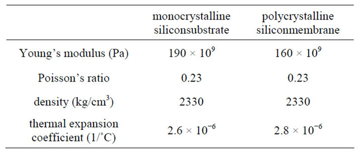
Table 1. Material properties of the monocrystalline substrate and the polysilicon membrane.
to be zero. The types of the loadings are considered as: pressure loadings and temperature loadings. The loading conditions are divided into three parts: applying temperature without pressure; applying pressure at room temperature (25˚C); and applying both pressure and temperature loadings. Under the above loading conditions, the effects and influences about the pressure and temperature to the membrane deformations can be analyzed. The values of the loading conditions are ranging from zero to 150 psi, and −10˚C to 75˚C for pressure and temperature respectively. Since the stress distributions caused by simply pressure loading, simply temperature loading, or both pressure and temperature loadings, the pressure and temperature distributions on the membrane of the pressure sensor can be known after the simulation. Furthermore, the best locations of the four inner piezoresistors can be obtained based on the maximum stress distribution to perform an effective output measurement indication.
3. Fabrication Process and Measurement
In this study, the fabrication of the proposed double Wheatstone-bridge pressure sensor is in comparison with the conventional single Wheatstone-bridge pressure sensor. Both the dimensions are  μm in length, width, and height respectively.
3.1. Fabrication of the MEMS-Based Pressure Sensors
In the fabrication process, the two types of sensors were patterned using the mask designs shown in Figures 3(a) and (b) respectively. Note that the patterning process was performed using cheaper film-photo masks with 30 μm line width and only two quartz masks with 1 μm line width respectively. As a result, it was found that the application of combining the two types of masks above reduced nearly 40% of the fabricating cost.
Figure 4 illustrates a schematic overview of the fabrication processes of the two types of pressure sensors, and the only difference is the choices of the mask patterns. In the beginning, a thin (20 μm) layer of polycrystalline silicon was deposit by the LPCVD technique on the surface of monocrystalline silicon substrate. The substrate was then located in the oxidation furnace at temperature 1092˚C and pressure 1 Pa for 30 hours to form a thin (800 Å) silicon oxide layers on the top and bottom surfaces of it shown in Figure 4(a). The substrate was then patterned using a photolithography technique, and immersed in a Buffered Oxide Etch (BOE) solution to remove the silicon oxide layer from the bottom surface. Partly of the silicon oxide layer from the top surface was also removed at the same time in order to create the designed basic outline of the piezoresistor structures shown in Figure 4(b). An ion-implantation method was then utilized to implant the polycrystalline silicon layer with boron to create the piezoresistor structures. In order to establish a resistance gradient within the structure, the light-ion implantation process was initially performed with 3.2 × 10¹⁴ atom/cm3 boron implant intensity to create a thin and high-resistance boron layer shown in Figure 4(c). After this procedure, the heavy-ion implantation process was performed with 1.5 × 10¹⁶ atom/cm3 boron implant intensity to create a thicker and low-resistance layer shown in Figure 4(d). Note that in both cases of the plating processes are performed by 80 KeV implantation energy. In the following procedure, the LPVCD technique was utilized to deposit the silicon nitride layers with a thickness of 1400 Å on the top and bottom surfaces of the substrate shown in Figure 4(e). A reactive ion etching (RIE) process was then performed to remove the silicon nitride layer from the top surface shown in Figure 4(f). After this, an aluminum layer with a thickness of 900 Å was sputtered on the top surface, patterned lithographically using AZ5214N photoresist, and etched at a temperature of 65˚C in H3PO4 acid to create the electrical Wheatstone-bridge circuits shown in