
Abstract
β-Ga2O3(010) homo-epitaxial growth was performed by plasma-assisted molecular beam epitaxy. Under Ga-rich conditions and for growth temperatures above 650 °C, the growth rate was independent of the Ga/O ratio (>1). A high growth rate of 2.2 nm/min for β-Ga2O3(010) was achieved by optimizing the O flux between 650 and 750 °C. Under Ga-rich conditions between growth temperatures of 500–900 °C, smooth surfaces with rms roughness below 1 nm were realized. We found that the slightly Ga-rich conditions between 650 and 750 °C were optimal for β-Ga2O3(010) growth with a smooth surface and a high growth rate.
Export citation and abstract BibTeX RIS
For high-power and high-temperature vertical electronic devices, β-Ga2O3 is one of the promising materials owing to its wide band gap (4.9 eV)1,2) and predicted high breakdown field (8 MV/cm).3) Bulk β-Ga2O3 can be grown by highly scalable, low-cost, melt-based methods,4–7) in comparison to other power-device materials, such as SiC, GaN, and diamond. Bulk β-Ga2O3 enables the growth of high-quality β-Ga2O3 epitaxial films. Recently, metal–oxide–semiconductor field-effect transistors (MOSFETs) of β-Ga2O3 homo-epitaxially grown by molecular-beam epitaxy (MBE) were demonstrated to have excellent properties.8) However, there are few reports of detailed investigations of β-Ga2O3 epitaxial growth, including those concerning its growth rate, growth mode, and crystalline quality. The clarification of the growth kinetics of β-Ga2O3 films will allow further improvements in β-Ga2O3 devices.
A β-Ga2O3 single crystal has a thermodynamically stable monoclinic structure (b-axis unique) belonging to the space group C2/m.9,10) The crystal structure of β-Ga2O3 has two crystallographically non-equivalent Ga positions (tetrahedrally and octahedrally coordinated) and two cleavage planes [(100) and (001)].10,11) The cleavage planes have a high decomposition rate in vacuum or in environments with low oxygen partial pressure, such as those realized in MBE systems, so that the epitaxial growth on the cleavage planes yields a low growth rate. High epitaxial-growth rates are desirable for the development of electron devices. The dependence of β-Ga2O3 growth rates on the growth planes was investigated in an MBE system using an  (
( ) gas mixture.12) The β-Ga2O3(100) cleavage plane was grown at a rate of 0.2 nm/min, while the β-Ga2O3(010) non-cleavage plane was grown at a substantially higher rate of >2 nm/min. The (010) non-cleavage plane is practical for β-Ga2O3 epitaxial growth.
For the β-Ga2O3(010) homo-epitaxial growth, an ozone MBE system was used. The ozone MBE system has the advantage of higher growth rates of β-Ga2O3(010) compared with a reported maximum rate of 10 nm/min.3) However, the precise control of the intentional doping densities in β-Ga2O3(010) films grown by an ozone MBE is difficult because of the high background pressure (>10−4 Torr). In our study, we used a plasma-assisted (PA) MBE system (PAMBE) with a comparatively lower background pressure of ∼10−5 Torr. In β-Ga2O3 growth using PAMBE, the Ga/O ratio influences the growth rate. In β-Ga2O3(100) growth, the growth rate decreases under metal-rich conditions as the stable Ga2O3 surface oxide is converted to a sub-oxide (Ga2O) with a high vapor pressure: Ga2O3 + 4Ga → 3Ga2O.13–15) Under Ga-rich conditions, the overall growth rate of Ga2O3 is limited by the competition between the Ga2O3 deposition and the Ga2O desorption. In this study, we systematically investigate the growth rate and growth mode of β-Ga2O3(010) films grown by PAMBE.
Sn-doped n-type β-Ga2O3(010) substrates (Tamura) were used for the growth studies presented here. For all substrates, the (010) surface was treated by chemical–mechanical polishing (CMP) and had an rms roughness of 0.1 nm over a 1 × 1 µm2 area. After solvent cleaning with acetone and isopropanol, the β-Ga2O3 substrates were indium bonded to a silicon backing wafer and subsequently baked at 220 °C for 2 h in ultra-high vacuum. On the β-Ga2O3(010) substrates, Ga2O3 was homoepitaxially grown using a Varian/Veeco 620 MBE system, equipped with an effusion cell to evaporate liquid Ga (99.99999%) and a Veeco Uni-Bulb RF plasma cell to produce active oxygen. Liquid Sn (99.9999%) was used as an n-type doping source of β-Ga2O3(010). Prior to the film growth, the elemental beam equivalent pressures (BEPs) of Ga and Sn were measured using a nude ion gauge located in the substrate position. For the oxygen plasma source, research-grade O2 gas (99.998%) was supplied through an in-line SAES pure gas dryer by an MKS pressure control module. Before the growth, an oxygen plasma treatment was carried out at a BEP of 1.2 × 10⁻⁵ Torr at 900 °C for 30 min to remove adsorbates from the substrate surface. We consider the internal thermocouple temperature near a heater behind the Si backing wafer as the growth temperature. Metallic Al (melting temperature 660 °C) on the Ga2O3 substrate melted at the thermocouple temperature of 645 °C. The surface morphologies and structures of the Ga2O3 layers were evaluated using atomic force microscopy (AFM; Veeco/Digital Instruments Dimension 3000) and reflection high-energy electron diffraction (RHEED), respectively. The RHEED measurements were conducted with an electron-beam energy of 7 keV.
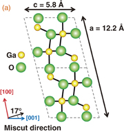
For the determination of the substrate vicinity (intentional or unintentional miscut), the crystal orientation was determined using high-resolution X-ray diffraction (XRD; X'pert PRO) by locating the (110) and (022) peak positions in a skew-symmetric geometry [inclined by 14.3 and 37.7° from (010), respectively]. This measurement revealed that the (100) plane could be cleaved most easily. The miscut components were determined by aligning the substrate surface parallel to the incident beam (measurements at 2θ = 0°), setting ω = 0°, and then determining the offset from 1/2(2θ)–ω to satisfy Bragg's law. The substrate was subsequently rotated by 90° about its surface normal and the procedure was repeated. The substrate miscut was 2.2° in a counterclockwise direction of 17° from the [001] direction (Fig. 1).
Download figure:
Standard image High-resolution image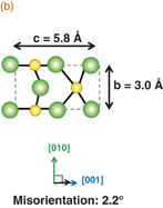
Fig. 1. Schematic illustrations of the unit cells of (a) the β-Ga2O3(010) surface and (b) the view along the [ ] direction. The large and small circles represent oxygen ions and gallium ions, respectively.
Download figure:
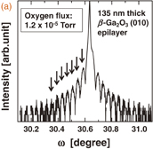
Standard image High-resolution imageThe growth rate of the β-Ga2O3(010) epitaxial films was determined using thickness fringes from XRD ω–2θ scans of the (020) diffraction plane. In wide-angular range 2θ–ω scans (2θ = 10–70°), the (010) and (020) diffraction peaks were detected, indicating that β-Ga2O3(010) single-crystal films were grown. The (020) ω–2θ scan diffraction peak of a 135-nm-thick β-Ga2O3(010) epitaxial film is shown in Fig. 2(a). Despite the homoepitaxial growth, up to 7th order satellite thickness fringes were clearly observed in high-resolution ω–2θ scans. The interface offsets are a result of a slight rigid-body displacement of the epitaxial film from the underlying substrate due to non-stoichiometry or impurities at the regrowth interface.16)
Download figure:
Standard image High-resolution image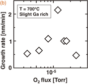
Fig. 2. (a) (020) ω–2θ scan diffraction peak of 135-nm-thick β-Ga2O3(010) film grown under slightly Ga-rich conditions ( ) with an oxygen flux of 1.2 × 10⁻⁵ Torr (BEP). (b) Relation of the growth rate of β-Ga2O3(010) at 700 °C under slightly Ga-rich conditions (
 ) to the oxygen flux (BEP).
Download figure:
Standard image High-resolution imageThe growth rate of the β-Ga2O3(010) films strongly depended on the O2 gas flux at a plasma power of 200 W [Fig. 2(b)]. At an oxygen flux of 1.2 × 10⁻⁵ Torr (BEP), the growth rate reached a peak of 2.2 nm/min. To establish which species were responsible for the growth, the emission of the oxygen plasma was measured by optical emission spectroscopy (OEM) from a viewport at the back of the oxygen plasma source. The light emission of the oxygen plasma displayed sharp peaks at wavelengths of 616, 777, and 845 nm, which are attributed to transitions of the excited oxygen.17) The flux of active atomic oxygen, or the oxygen plasma emission intensities, should have a strong influence on the growth rate of β-Ga2O3 by PAMBE. However, at a plasma power of 200 W, the oxygen plasma emission intensities continuously increased with an increasing O2 gas flux from 0.4 to 2.9 × 10⁻⁵ Torr (BEP), i.e., there was no peak in the plasma emission intensities for the O2 gas flux. The plasma emission intensity was measured not from a substrate surface, but from the back side of the oxygen plasma source. Further investigation is required to clarify the specific active atomic oxygen fluxes at the substrate surface. Attempts to grow β-Ga2O3 with the same oxygen flow but with the plasma source turned off were unsuccessful, i.e., the growth of β-Ga2O3(010) required active atomic oxygen from the plasma source. For the remaining growth processes, the rf plasma power and oxygen flux were maintained at 200 W and 1.5 × 10⁻⁵ Torr, respectively, corresponding to 1 nm/min of O* flux. 1 nm/min is equivalent to 0.11 monolayer (ML)/s, where 1 ML of Ga2O3(010) corresponds to b/2 = 0.15 nm.
The RHEED patterns of the β-Ga2O3(010) substrate surfaces are shown in Fig. 3. With a 104° substrate rotation, the RHEED patterns were observed along the [100] and [001] azimuths. Because of the small miscut (<0.5°) parallel to the [100] direction, the RHEED pattern exhibited vertical rods for the [001] azimuth [Fig. 3(a)]. The as-received substrate had vague streaky 1 × 2 RHEED patterns [Fig. 3(a)], while after the oxygen plasma treatment the surface had the streaky 1 × 2 RHEED patterns associated with smooth surfaces [Fig. 3(b)]. During growth under temperatures lower than 450 °C, the 1 × 2 RHEED patterns became spotty, indicating that growth temperatures above 450 °C are required for a smooth surface. The other surface reconstruction was not observed during or after growth. The RHEED intensity oscillation was not observed during the growth, indicating a continuous step-flow growth mode due to a large miscut angle. The realization of a layer-by-layer growth mode requires on-axis substrates which have sufficiently large terrace widths to enable island formation. After opening the Ga and O* plasma shutter at growth temperatures below 600 °C under Ga-rich conditions, the RHEED intensity sharply decreased with decreasing growth temperature [Fig. 3(c)]. We propose that excess Ga adlayers on the β-Ga2O3(010) surface exist under Ga-rich conditions, causing an increase in diffuse scattering. For growth temperatures above 600 °C, the RHEED intensity was constant, which was attributed to desorption of excess Ga from the surface.
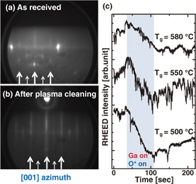
Fig. 3. RHEED patterns of (a) as-received and (b) plasma-cleaned β-Ga2O3(010) substrate surfaces at an oxygen flux of 1.2 × 10⁻⁵ Torr at 600 °C for 30 min. (c) RHEED intensity dependence on time for low growth temperature <600 °C.
Download figure:
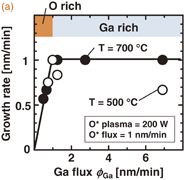
Standard image High-resolution imageTo calibrate the Ga flux (ΦGa) and the O* flux ( ) in Ga2O3 growth-rate units (nm/min), we used thickness fringes from XRD ω–2θ scans of the (020) diffraction plane for Ga2O3 grown under Ga- and O-limited conditions, respectively.18) The dependence of the Ga2O3 growth rate on an impinging Ga flux at T = 500 and 700 °C is shown in Fig. 4(a). Under Ga-limited conditions (
 ), the growth rate at T = 500 and 700 °C proportionally increased with the Ga flux, indicating that the impinging Ga flux was incorporated into the Ga2O3 films. At T = 700 °C, the growth rate reached a peak at 1 nm/min under stoichiometric conditions (
 ) and remained at 1 nm/min for Ga-rich conditions (
 ). At T = 700 °C under metal rich conditions [e.g., up to ΦGa (= 20 nm/min)], no Ga droplets were observed on the sample surface. This was consistent with a constant RHEED intensity during growth above 600 °C for metal-rich growth. We attribute the constant streaky RHEED pattern for metal-rich growth at high temperatures to a continuous step-flow or step-flow-like growth without the formation of Ga metal droplets on the surface. Presumably, excess Ga adatoms desorbed from the β-Ga2O3(100) surface for T > 600 °C. Surprisingly, the growth rate at T = 500 °C decreased with increasing Ga flux. Low temperature β-Ga2O3 growth shows similar tendencies as β-Ga2O3(100) growth,15) in which excess Ga adatoms form the volatile Ga2O sub-oxide and reduce the growth rate under Ga-rich conditions. Although speculative, we believe that the residency time for excess Ga on the (010) surfaces at high temperatures (>600 °C) was short enough for the direct desorption of Ga, whereas at lower temperatures the reaction of excess Ga with activated oxygen favored the formation of the volatile Ga2O sub-oxide.
Download figure:
Standard image High-resolution image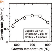
Fig. 4. (a) Relation of the growth rate of β-Ga2O3(010) via impinging Ga flux ΦGa at 500 °C (black circles) and 700 °C (white circles). The oxygen plasma power and flux were 200 W and 1.5 × 10⁻⁵ Torr, respectively, corresponding to an O* flux of 1 nm/min. (b) Growth rate of β-Ga2O3(010) under slightly Ga-rich conditions ( ) as a function of growth temperature. The oxygen flux was 1.5 × 10⁻⁵ Torr.
Download figure:
Standard image High-resolution imageThe growth rate dependence on the growth temperature under slightly Ga-rich conditions ( ) is shown in Fig. 4(b). For a growth temperature between 650 and 750 °C, the growth rate was constant at 1 nm/min. For T > 750 °C, the growth rate decreased with increasing growth temperature and was independent of the Ga/O ratio (>1). We assume that the reduced growth rate at a high growth temperature resulted from the decomposition of the β-Ga2O3(010) films. For T < 650 °C, the growth rate was reduced with decreasing growth temperature, yielding a low growth rate at 500 °C under slightly Ga-rich conditions [Fig. 4(a)]. As mentioned above, the RHEED intensity continuously decreased during growth under Ga-rich conditions for T < 600 °C. We consider that the excess Ga adlayer for T
  600 °C prevents oxygen atoms from incorporating into the Ga2O3 films, resulting in the reduction of the growth rate. Another possibility is the formation of volatile gallium sub-oxides (Ga2O). For T < 600 °C, the excess Ga reacts with Ga2O3 surface oxides, resulting in the formation and desorption of Ga2O. However, for T
  600 °C, the excess Ga can be desorbed from the surface without the formation of Ga2O. To verify the mechanisms responsible for the reduced growth rate at low and high growth temperatures, further studies are planned using line-of-sight quadrupole mass spectroscopy (QMS).19)
The surface morphologies of ∼60-nm-thick β-Ga2O3(010) films are shown in Fig. 5. For T < 900 °C, the Ga2O3 layer had a smooth surface. The rms roughness in Figs. 5(a), 5(b), 5(c), and 5(d) was 0.1, 0.3, 0.6, and 0.1 nm, respectively, over 1 × 1 µm2. The smooth surface of the β-Ga2O3(010) films may be attributed to the step-flow growth mode due to the large miscut angle (>2°) of the substrate. The surface morphology and roughness were insensitive to the Ga/O ratio, indicating a large growth window for a smooth surface. From these results, we conclude that slightly Ga-rich conditions between 650 and 750 °C are suitable for obtaining smooth surfaces with a high growth rate.
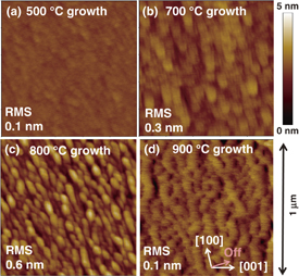
Fig. 5. Surface morphologies of ∼60-nm-thick β-Ga2O3(010) layers grown on Sn-doped β-Ga2O3(010) on-axis substrates at a growth rate of 1 nm/min (oxygen flux of 1.5 × 10⁻⁵ Torr) under slightly Ga-rich conditions ( ). The growth temperatures were (a) 500, (b) 700, (c) 800, and (d) 900 °C.
Download figure:
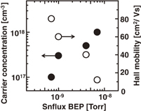
Standard image High-resolution imageHall measurements were performed at room temperature on 300-nm-thick Sn-doped β-Ga2O3(010) films with various Sn BEPs (7 × 10⁻¹⁰–7 × 10⁻⁹ Torr) using 150 × 150 µm2 van der Pauw (vdP) patterns. In PAMBE, the Sn flux could be stably controlled by the cell temperature. The Sn-doped β-Ga2O3(010) homoepitaxial films were electrically isolated by 50-nm-thick undoped β-Ga2O3(010) films with high resistivity and had no SnO2 peaks in XRD 2θ–ω scans. An Ohmic contact was achieved by BCl3 reactive ion etching prior to the fabrication of Ti (20 nm)/Au (200 nm) metal stacks annealed at 500 °C for 1 min in N2.3) The relation of the Hall carrier concentration and Hall mobility to the Sn BEP is shown in Fig. 6. The carrier concentration and mobility of the Sn-doped β-Ga2O3(010) epitaxial films were around 1 × 1017 cm2 and 80 cm2 V−1 s−1, respectively. This is comparatively close to the values of Sn-doped β-Ga2O3(010) films grown by ozone MBE.12)
Fig. 6. Carrier concentration and Hall mobility dependence of 300-nm-thick Sn-doped β-Ga2O3(010) epitaxial films on Sn flux (BEP) at room temperature. The black and white circles show the carrier concentration and Hall mobility, respectively.
Download figure:
Standard image High-resolution image
In conclusion, we grew homoepitaxial β-Ga2O3(010) layers using PAMBE. A high growth rate of 2.2 nm/min was achieved for β-Ga2O3(010) by optimizing the O2 flux, Ga/O ratio, and growth temperature. Under Ga-rich conditions for T < 650 °C, the growth rate decreased with decreasing growth temperature, while for T > 750 °C, the growth rate decreased with increasing growth temperature. Slightly Ga-rich conditions between 650 and 750 °C are optimal for a smooth surface with an rms surface roughness of 0.1 nm at a high growth rate.
Acknowledgments
The authors acknowledge J. H. English for MBE advice and E. Young for supporting off-angle and orientation measurements using XRD. This work was supported by the MRSEC Program of the National Science Foundation under Award No. DMR 1121053. Additionally, the first author is thankful to JSPS Postdoctoral Fellowships for Research Abroad.