

Abstract
We analyze the structural-asymmetry-induced nonlinear enhancement of the electron mobility μ in a GaAs/InxGa1−xAs double-quantum-well pseudomorphic high-electron-mobility transistor (p-HEMT). We consider the well widths wi and ws and the doping concentrations ndi and nds in the barriers along the substrate (inverted doping) and surface (surface doping), respectively. We show that for a suitable choice of ws and nds, the variation of wi leads to interesting changes in the occupation of subbands, i.e., first, single-subband, then double-subband, and again, single-subband occupancy. By increasing ndi, the range of double-subband occupancy is enhanced. However, the lowering of μ due to the inter-subband effects is minimized. In the case of a single-channel HEMT, i.e., say, for ndi = 0, only a single subband is occupied. The mobility exhibits a cusplike behavior with a minimum at a certain value of wi. If one takes a higher value of nds, the occupation of subbands shows a different trend, i.e., from single- to double-subband occupancy as a function of wi for different ndi values with nonmonotonic variations of μ. Our results of the nonlinear enhancement of mobility can be utilized for the analysis of the coupled GaAs/InxGa1−xAs double-quantum-well p-HEMT structure.
Export citation and abstract BibTeX RIS
1. Introduction
The pseudomorphic high-electron-mobility transistors (p-HEMTs) based on the InGaAs heterostructure are highly important because of their application in the microwave and millimetre frequency ranges, which are suitable for defence and commercial applications.1) The p-HEMT structures exhibit high power gain, excellent cut-off frequency, low noise, and extremely good dc characteristics suitable for power microwave and high-speed device applications.2–9) The performance of a device depends on the improvement of sheet electron density and mobility. Much effort has been made to study the enhancement of the electron mobility in the InGaAs-based pseudomorphic channels by employing different structure geometry and doping profiles.10–15)
A double quantum well is an interesting system because of the occurrence of tunneling coupling in addition to the quantum confinement of the carriers.16,17) When two separate wells are brought closer to each other, their subband wave functions overlap through the central barrier, leading to the splitting of the subband energy levels. If the well widths are equal and also the doping concentrations have symmetric profiles, a symmetric coupled potential structure can be obtained in which the subband wave functions extend into both the wells equally. The lowest (bonding) and first excited (antibonding) wave functions exhibit completely symmetric and antisymmetric behaviors, respectively. However, the slight variations of the well widths or doping concentrations disturb the symmetry of the structure so that the resonance of the subband states is destroyed. As a result, an asymmetric double quantum well is formed, in which one of the two lowest subband wave functions almost lies in one well, while the other wave function lies in another well.16,17) By varying the structure parameters or by applying an external electric field, the subband wave functions can be displaced from one well to the other.16–18) The asymmetry of the structure parameters affects the optical properties of pseudomorphic double quantum wells substantially.19–23)
In this work, we analyze the electron mobility as a function of the asymmetry of the structure parameters of a strained GaAs/InxGa1−xAs double quantum well. We consider that the barriers, lying towards the substrate and surface sides, are delta-doped with different doping concentrations, ndi and nds, respectively. The corresponding well widths are also made unequal as wi and ws. We calculate the subband energy levels and wave functions by using self-consistent solutions of the Schrödinger and Poisson's equations. The variations of the structure parameters change the subband energy levels, wave functions, and also the occupation of subbands. As a result, the scattering potentials are affected, thereby changing μ. In the case of more than one subband occupancy, their influence on the scattering potentials is mediated through the inter-subband effects. We consider the scatterings due to the ionized impurities (imp-), alloy disorder (al-), and interface roughness (ir-) to calculate μ. We use the random phase approximation to screen the scattering potentials. We show that the asymmetric combinations of doping concentrations and well widths lead to the interesting variations of the occupation of subbands. For example, when nds and ws remain unchanged, the occupations of subbands vary from single to double and then again single-subband occupancy as a function of wi. The nonlinearity of μ due to the transition of the occupation of subbands can be regulated by varying ndi. For ndi = 0, only the single subband is occupied with a cusplike variation of μ about a certain value of wi having a faster rise towards higher values of wi. By considering an increased value of nds, there is single-to double-subband occupancy only. For a low wi, under the single-subband occupancy, the mobility increases with the increase in ndi. However, for a larger wi, the variations of μ for different ndi values are different. We show that the nonlinear variation of mobility for different asymmetric combinations of well widths and doping concentrations is mostly due to the variations of the subband mobilities through changes in the scattering rate matrix elements due to the shifting of subband wave functions between the wells. In Sect. 2, we present the theory for the calculations. In Sect. 3, we discuss the results, while in Sect. 4, we provide a summary.
2. Theory
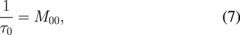
We consider the GaAs/InxGa1−xAs double-quantum-well HEMT structure shown in Fig. 1. The InxGa1−xAs well layers of widths wi and ws are separated by a thin GaAs barrier of width b, thereby allowing the coupling of eigenstates of the two wells. The GaAs side barriers are delta-doped with Si of widths d and doping concentrations ndi and nds at the spacer distance s from the interfaces along the substrate and surface sides of the structure, respectively. The transferred electrons in the wells interact with the ionized donors in the side barriers through Coulomb interaction, leading to band bending. The electrons are thus confined in the wells near the outer interfaces, leading to a coupled two-dimensional electron gas (2DEG).24,25) The doping concentrations perpendicular to the interface plane can be written as
One can also write the electron concentration distribution n(z) of the coupled system as24)

The summation over n stands for different subbands and nn is the number of electrons per unit area in the nth subband. The confinement potential V(z) = VH(z) + VS(z), where VH(z) is the Hartree potential responsible for band bending and VS(z) is the structure potential, which takes care of band offset near interfaces. VH(z) can be obtained by solving Poisson's equation,24)

where ε0 is the dielectric constant. Within the effective mass approximation, the electron subband wave functions ψn(z) corresponding to the energy eigenvalues En satisfy the one-dimensional Schrödinger equation along the z-direction.24)
We adopt the self-consistent solution of the one-dimensional Schrödinger and Poisson's equations to obtain ψn(z), En, and nn.
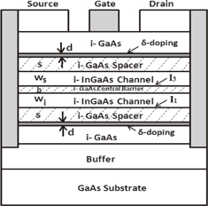
Fig. 1. Schematic diagram of the strained GaAs/InGaAs asymmetric double-quantum-well HEMT structure with well widths wi and ws (Å), barrier width b (Å), spacer width s (Å), and Si delta-doped layers of width d (Å).
Download figure:
Standard image High-resolution imageThe subband transport lifetime τn can be written as τn = τn (EFn) since the electrons on the Fermi surface contribute to transport at the temperature T = 0 K. EFn = EF − En is the Fermi energy of the nth subband, where EF is the Fermi energy. EFn is related to the 2D electron density of the nth subband,24)

where θ is the Heaviside step function. The surface electron density Ns can be expressed in terms of nn as24)
where N is the number of filled levels.
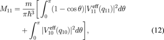
We obtain the multi-subband transport lifetime τn, which satisfies a coupled linear equation, by using the Boltzmann transport equation.24,25) We consider occupancy up to two lowest subbands. Under double-subband occupancy, the inter-subband interaction plays a major role in the calculation of the subband lifetime.26–30) In the case of the single lowest subband occupancy (n = 0), τ0 can be written as24)
where
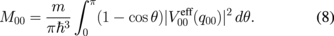
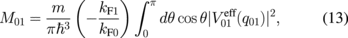
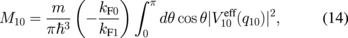
However, when the two lowest subbands are occupied (n = 0, 1), the subband life times τ0 and τ1 can be written as \int_{0}^{\pi }d\theta \cos \theta |V_{10}^{\text{eff}}(q_{10})|^{2} $](https://content.cld.iop.org/journals/1347-4065/56/6/064101/revision1/RP170050if023.gif) s.24)
s.24)
where

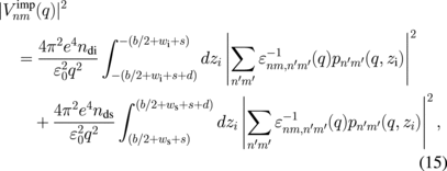
![$q_{n1} = [k_{\text{F}n}^{2} + k_{\text{F}1}^{2} - 2k_{\text{F}n}\ k_{\text{F}1}\cos \theta ]^{1/2}$](https://content.cld.iop.org/journals/1347-4065/56/6/064101/revision1/RP170050if024.gif) , and kFn = (2mEFn/ħ2)1/2. We consider nonphonon scattering mechanisms due to ionized impurities, interface roughness, and alloy disorder. We adopt the random phase approximation to screen the scattering potentials. The screened ionized impurity scattering potential can be written as
, and kFn = (2mEFn/ħ2)1/2. We consider nonphonon scattering mechanisms due to ionized impurities, interface roughness, and alloy disorder. We adopt the random phase approximation to screen the scattering potentials. The screened ionized impurity scattering potential can be written as
where

The screened interface roughness scattering potential can be written as
Similarly, the screened alloy disorder scattering potential can be written as
 is the inverse of the dielectric screening matrix.24) In practical numerical calculations, the sums over n', and m' are normally considered to be over the occupied subbands.30) Impurity scattering is responsible for this owing to the ionized impurities lying in the side barriers. Alloy scattering arises from the InxGa1−xAs wells, unlike the GaAs/AlxGa1−xAs structures, where it occurs from the barrier regions.25) Interface roughness scattering is assumed to occur from the interfaces lying towards the substrate side.26,29,30) ZI is the position corresponding to the interfaces I1 and I3, which are considered as rough (Fig. 1). Note that, when the double subband is occupied, the expression for M00 [Eq. (11)] contains an additional (inter-subband) term compared with that in Eq. (8). We also note that the contribution of the intra-subband term [first term in Eq. (11)] is also different from that in Eq. (8) through the dielectric screening matrix because of the change in the occupation of subbands. The subband transport lifetime τnimp/ir/al can be related to the subband transport mobility μnimp/ir/al, where μnimp/ir/al = (e/m*)τnimp/ir/al. The mobility due to a particular scattering mechanism (imp/ir/al) can be calculated as

We adopt Matthiessen's rule to calculate the total mobility μ.24)
3. Results and discussion
We study the effects of the asymmetric variations of well widths and doping concentrations on the multi-subband electron mobility of the strained GaAs/In0.2Ga0.8As double-quantum-well structure. The potential barrier height V0, which depends on the conduction band offset, is obtained from the strain-dependent band gap between InxGa1−xAs and GaAs. For the mole fraction x = 0.2, V0 = 140 meV.31) The strain-dependent electron effective mass m is 0.62 m0.32) The interface roughness parameters are the mean height of the roughness, Δ = 2.83 Å, and the correlation length Λ = 100 Å. The alloy disorder scattering potential δV is 530 meV.26) We consider the spacer width s = 100 Å, the doping layer width d = 20 Å, and the central barrier width b = 60 Å.
We study the mobility as a function of asymmetry in well widths by considering ws = 100 Å and varying wi. The doping profiles are made symmetric, ndi = nds = 0.25 × 1018 cm−3. The mobility of the individual scattering mechanisms, μimp/ir/al, and the total mobility μ (cm2 V−1 s−1) are presented in Fig. 2 as a function of wi (Å). With the increase in wi, the occupation of subbands changes from single to double, and then again, single-subband occupancy. Near the transition of occupation of subbands, a discontinuity in mobility occurs owing to inter-subband effects. There are abrupt drops (rises) in μ, μimp, and μir near the transition from single- to double- (double- to single-) subband occupancy. The discontinuity in μimp is more than that in μir. On the other hand, note that the change in μal has an opposite trend. With the increase in wi, μ almost increases. Under the double-subband occupancy, μ is mostly governed by imp-scattering. For smaller well widths (wi < 90 Å), when a single subband is occupied, the mobility is governed by all the scattering mechanisms, imp-, al-, and ir-scatterings, whereas towards larger wi values (wi > 90 Å), the effect of ir-scattering is minimized.
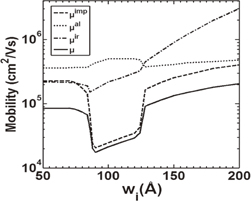
Fig. 2. Mobility due to individual scattering mechanisms, μimp/ir/al, and total mobility μ as a function of wi for ws = 100 Å and ndi = nds = 0.25 × 1018 cm−3.
Download figure:
Standard image High-resolution imageIn Fig. 3, we present the subband mobilities μ0imp/ir/al and μ1imp/ir/al as a function of wi to explain the difference between the changes in μimp, μir, and μal at the transition of occupation of subbands as described in Fig. 2. We note that the drop in μ0imp is more than that in μ0ir near the change in occupation from single- to double-subband occupancy. In the case of μ0al, the lowest drop is observed. Regarding μ1imp/ir/al, it manifests within the double-subband occupancy. There is a marked variation among different subband mobilities as a function of wi mediated by inter-subband effects. For imp-scattering, μ1imp starts from zero, becomes maximum, and then decreases such that μ0imp ≫ μ1imp. On the other hand, in the case of ir- and al- scatterings, μ1ir/al is substantial and of the same order of μ0ir/al. This difference in the variation of subband mobilities, μ0imp/ir/al and μ1imp/ir/al, is based on the change in scattering potential through the dielectric screening matrix involving the intra- and inter-subband terms [Eqs. (15)–(18)]. As a result, there are net drops in μimp and μir, but a small rise in μal near the transition from single- to double-subband occupancy. The discontinuity in mobility near the transition from double- to single-subband occupancy can similarly be analyzed.
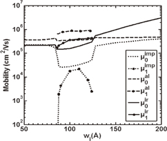
Fig. 3. Subband mobilities μ0imp/ir/al and μ1imp/ir/al as a function of wi for ws = 100 Å and ndi = nds = 0.25 × 1018 cm−3.
Download figure:
Standard image High-resolution imageIn Fig. 4, we present μ as a function of the well width by considering symmetric well widths, wi = ws, but considering asymmetric doping concentrations, i.e., ndi = 0.0, 0.25, 0.5, 1.0, and 2.0 × 1018 cm−3 for a fixed nds (nds = 1.0 × 1018 cm−3). We note that for ndi = 0, the variation of wi facilitates the occurrence of single-subband then double-subband and again single-subband occupancy as a function of wi as in Figs. 2 and 3. However, for all other doping concentrations, the double subband is occupied in the entire wi range. In general, as the doping concentration increases, the mobility increases as long as the occupation of subbands remains unchanged. In the inset of Fig. 4, we present μimp/ir/al for ndi = 0 and nds =1.0 × 1018 cm−3. For the entire wi range, al- and imp-scatterings dominate the mobility, except in the smaller well width range (w < 70 Å), where the contribution of ir-scattering is effective. Unlike the GaAs/AlxGa1−xAs systems, here in the GaAs/InxGa1−xAs structures, al-scattering contributes substantially since the channel layer is an alloy.
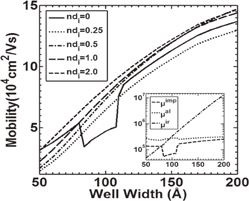
Fig. 4. Mobility μ as a function of the well width, obtained by considering wi = ws, nds = 1.0 × 1018 cm−3, and ndi = 0.0, 0.25, 0.5, 1.0, and 2.0 × 1018 cm−3.
Download figure:
Standard image High-resolution imageIn Fig. 5, we vary both well widths and doping concentrations and present μ (cm2 V−1 s−1) as a function of wi (Å) for ws = 100 Å and nds = 0.25 × 1018 cm−3, considering different values of ndi (ndi = 0.0, 0.25, 0.5, 1.0, and 2.0 × 1018 cm−3). As ndi increases, the asymmetry between the doping concentrations increases. The well width range for the occurrence of double-subband occupancy increases. However, the magnitude of drop in mobility near the transition of occupation of subbands decreases. For ndi ≥ 1 × 1018 cm−3, the double subband is occupied even at wi = 60 Å. In the case of ndi = 0, there is single-subband occupancy throughout the entire wi range with a dip in mobility around wi = 110 Å. Unlike the other mobility curves, where inter-subband effects play a role in determining μ, here, in the case of ndi = 0, the mobility is governed by the lowest intra-subband scattering, mostly imp-scattering. To explain the dip in mobility, we note that the variation of wi changes the structure potential. Around wi = 110 Å, the resonance of subband states and hence the minimum of anticrossing of subband energy levels occur. Accordingly, the Fermi energy level of the lowest subband EF0 has a minimum around wi = 110 Å. Since the imp-scattering potential [Eq. (15)] is inversely proportional to EF0, the mobility is being affected through the intrasubband scattering [Eq. (7)]. We further note that, around the resonance, the distribution of subband wave functions varies considerably.24–26) The lowest subband wave function ψ0, which almost lies in the right well for wi < 110 Å, is pushed towards the left well when wi > 110 Å, leading to a decrease in the effect of the imp-scattering potential. Therefore, the net effect of the above two mechanisms leads to a dip in mobility around wi = 110 Å with a small increase for wi < 110 Å but a large increase towards wi > 110 Å.
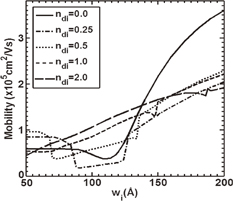
Fig. 5. Mobility μ as function of wi (Å) for ws =100 Å, ndi = 0.0, 0.25, 0.5, 1.0, and 2.0 (× 1018 cm−3), and nds = 0.25 × 1018 cm−3.
Download figure:
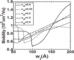
Standard image High-resolution imageIn Fig. 6, we present μ (cm2 V−1 s−1) as function of wi (Å) for ws = 100 Å and ndi = 0.0, 0.25, 0.5, 1.0, and 2.0 (× 1018 cm−3) by considering a higher value of nds (nds =1.0 × 1018 cm−3) compared with Fig. 5. As in the earlier case (Fig. 5), here, also a single subband is occupied from the beginning of wi, i.e., at wi = 50 Å for ndi = 0, 0.25, and 0.5 × 1018 cm−3. The mobility increases with the increase in ndi. The change from single- to double-subband occupancy occurs at a decreased value of wi with the increase in ndi. For ndi =1.0 and 2.0 (× 1018 cm−3), two subbands are occupied at wi = 50 Å. However, unlike in Fig. 5, here, no change from double-subband to single-subband occupancy is obtained. This is because the larger band bending due to the higher nds also leads to double-subband occupancy at larger wi values.
Fig. 6. Mobility μ as function of wi (Å) for ws = 100 Å, nds = 1.0 × 1018 cm−3, and ndi = 0.0, 0.25, 0.5, 1.0, and 2.0 (× 1018 cm−3).
Download figure:
Standard image High-resolution image
We note that the decrease in mobility at the onset of the occupation of the second subband also causes the decrease in the current since the surface electron density Ns, which is the sum of the electron densities of the occupied subbands, remains unchanged [Eq. (6)]. This trend in the change in the current is also maintained by varying the well widths since the increase in the well width causes only the overall increase in the mobility owing to the reduction in the effect of the scatterers.
4. Conclusions
The principal work involved in this paper is to relate the enhancement of electron mobility to the asymmetric variations of the structure parameters in a GaAs/InxGa1−xAs double-quantum-well pseudomorphic high-electron-mobility transistor (p-HEMT). We calculate the subband energy levels and wave functions through the self-consistent solution of the Schrödinger and Poisson's equations and use them to determine the electron mobility for the multi-subband occupied system. We show that suitable choices of well widths and doping concentrations lead to interesting changes in the occupation of subbands causing nonlinear trends in mobility through intersubband effects. The nonlinearity in the mobility depends on the changes in the scattering potentials due to the shifting of the subband wave functions from one well to the other because of the asymmetric variations of the structure parameters. Our results can be utilized for the analysis of the device performance of GaAs/InxGa1−xAs coupled double-quantum-well p-HEMT structures.