

Abstract
The homoepitaxial growth of thick β-Ga2O3 layers on 2-in.-diameter (001) wafers was demonstrated by halide vapor phase epitaxy. Growth rates of 3 to 4 µm/h were confirmed for growing intentionally Si-doped n-type layers. A homoepitaxial layer with an average thickness and carrier concentration of 10.9 µm and 2.7 × 1016 cm−3 showed standard deviations of 1.8 µm (16.5%) and 0.5 × 1016 cm−3 (19.7%), respectively. Ni Schottky barrier diodes fabricated directly on a 5.3-µm-thick homoepitaxial layer with a carrier concentration of 3.4 × 1016 cm−3 showed reasonable reverse and forward characteristics, i.e., breakdown voltages above 200 V and on-resistances of 3.8–7.7 mΩ cm2 at room temperature.
Export citation and abstract BibTeX RIS
Beta gallium oxide (β-Ga2O3) has a large bandgap of 4.5–4.9 eV and at the same time can be made conductive by doping with donor impurities. It follows from these properties that β-Ga2O3 has a wide range of applications, such as being used as transparent and conductive substrates for nitride-based LEDs,1) a new material for deep-UV photodetectors,2) or high-power devices.3,4) On the other hand, bulk single crystals of β-Ga2O3 can be grown by using melt growth methods at atmospheric pressure.5–9) Considering the cost-effectiveness, this is a big advantage of β-Ga2O3 over other wide-bandgap semiconductor materials such as SiC and GaN whose bulk crystal growth is limited to gas-phase methods, which means that the growth rates are relatively low. Our group has developed high-quality bulk single crystals of β-Ga2O3 by the edge-defined film-fed growth (EFG) method, and wafers based on these bulk crystals have already been commercialized.9) Furthermore, the electrical conductivity of the bulk crystals can be controlled by doping with Sn/Si or Fe/Mg, making the material conducting or semi-insulating, respectively.
Research and development activities on power devices using β-Ga2O3 material have also shown much progress recently. Superior device performances have been reported for Schottky barrier diodes (SBDs)10–13) and field-effect transistors (FETs).14,15) For example, breakdown voltages larger than 1000 and 750 V have been achieved respectively in field-plated β-Ga2O3 SBDs11) and MOSFETs.14) In vertical power devices such as SBDs where n−-β-Ga2O3 thick layers are used as the drift layers, a thickness of some micrometers and a doping concentration on the order of 1016 cm−3 are typically required. To this end, halide vapor phase epitaxy (HVPE) has proved to be an effective method of growing thick and high-purity epitaxial layers of β-Ga2O3 owing to its high growth rate and efficient impurity doping controllability. The growth rate that can be obtained is as high as 5–20 µm/h.16,17) Moreover, the n-type carrier concentration can be controlled in the range of 1016–1018 cm−3 by introducing Si as the donor. The present lower limit of doping is nearly the same as that in MBE-grown β-Ga2O3 layers18) but one order of magnitude lower than that in MOVPE-grown ones.19)
In this study, we report on the homoepitaxial growth of β-Ga2O3 on 2-in.-diameter (001) wafers by HVPE, which was successfully performed for the first time. Following the enlargement of the wafer sizes, this scaling-up technology for the epitaxial growth has always been desirable towards the commercialization of β-Ga2O3 devices.
650-µm-thick 2-in.-diameter (001) β-Ga2O3 wafers prepared by EFG with n-type conductivity [effective donor concentration, Nd − Na, (3–4) × 1018 cm−3] by Sn doping20) were used as substrates. Prior to homoepitaxial growth, the wafers were subject to degreasing in organic solvents followed by cleaning in hydrofluoric acid and in a mixture of sulfuric acid and hydrogen peroxide solutions. The epitaxial layers were then grown in a horizontal hot-wall HVPE reactor with GaCl and O2 as precursors, SiCl4 as doping gas, and N2 as a carrier gas. The choice of precursors was based on the thermodynamic analysis of the driving force for β-Ga2O3 growth.16) The reactor was scaled up from that in Ref. 17, which was designed for smaller samples (10 × 22 mm2). The Ga precursor, namely, GaCl is generated in situ by the reaction between high-purity Ga metal (7N grade) and Cl2 gas in the so-called source zone maintained at 850 °C. β-Ga2O3 is then grown by the reaction between GaCl and O2 gas in the growth zone. The temperature of the growth zone was set at 1000 °C. Note that no wafer rotation mechanism is employed in the HVPE reactor used.
The structural quality of the grown layers was characterized by the full-widths at half-maximum (FWHMs) of X-ray rocking curves (XRCs) for symmetric 002 reflection with X-ray incident azimuth of [100]. The thickness and carrier concentration (Nd − Na) of the grown layers were measured by Fourier transform infrared spectroscopy (FT-IR) and electrochemical capacitance–voltage (ECV) measurements. As for the relative dielectric constant of β-Ga2O3, a value of 1021) was used for the estimation of carrier concentration in ECV measurement.
HVPE of β-Ga2O3 layers was successfully achieved on 2-in.-diameter wafers with a typical growth rate of 3–4 µm/h for a GaCl nominal input partial pressure of 1.3 × 10⁻³ atm and an input VI/III (2O2/GaCl) ratio of 3.5. Figure 1 shows a photograph of a homoepitaxial wafer after HVPE growth for 3 h and subsequent surface planarization by chemical mechanical polishing (CMP). The FWHMs of (002) XRCs taken at five sampling points were 89–100 arcsec. These values are comparable to that of the wafer measured at the center, which is 125 arcsec, implying the high crystalline quality of the homoepitaxial layer. The distributions of thickness and carrier concentration of the same homoepitaxial wafer obtained before CMP are shown in Fig. 2. The data was taken at 25 sampling points and has been smoothened for the points in between as displayed in the figures. The upstream edge (left-hand side of the figure) is relatively thin (minimum thickness ∼4.5 µm) compared with the remaining part (9.3–12.3 µm). This is attributed to the nonoptimized gas flow condition (i.e., nonuniform gas velocity and/or distribution of precursors over the wafer surface). The mean values and standard deviations (mean ± σ) for thickness and carrier concentration were 10.9 ± 1.8 µm and (2.7 ± 0.5) × 1016 cm−3, respectively. The inhomogeneity (defined as σ/mean) is 16.5% for thickness and 19.7% for carrier concentration. These values are larger than desirable since a value of 2–3% inhomogeneity for thickness is obtained for the state-of-the-art 6-in.-diameter 4H-SiC22) and GaN23) homoepitaxial layers. However, the uniformity is expected to be improved by optimizing the gas flow and/or utilizing the wafer rotation mechanism in future studies.
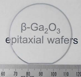
Fig. 1. Photograph of a 2-in.-diameter (001) β-Ga2O3 wafer after 3 h growth of homoepitaxial layer by HVPE and subsequent planarization of the grown layer surface by CMP.
Download figure:
Standard image High-resolution image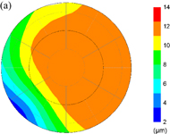
Download figure:
Standard image High-resolution image
Fig. 2. Distributions of (a) thickness and (b) carrier concentration of an as-grown Si-doped (001) β-Ga2O3 homoepitaxial layer grown by HVPE on a 2-in.-diameter wafer for 3 h.
Download figure:
Standard image High-resolution imageTo examine the quality of the homoepitaxial wafers prepared, SBDs were fabricated on a 2-in.-diameter homoepitaxial wafer. The homoepitaxial layer was planarized by CMP prior to the device process to remove pits formed on the surface.12) The nominal thickness and average carrier concentration of the homoepitaxial layer after the CMP procedure were 5.3 µm and 3.4 × 1016 cm−3, respectively. Ti (50 nm)/Au (200 nm) cathode metals were then deposited on the back of the substrate by electron-beam evaporation to form ohmic contact over the entire area. Finally, circular Schottky contacts consisting of Ni (50 nm)/Au (200 nm) with various diameters (50–1000 µm) were deposited on the homoepitaxial layer via a photolithography process. A photograph of SBDs fabricated on the homoepitaxial wafer is shown in Fig. 3.
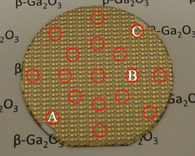
Fig. 3. Photograph of SBDs fabricated on a 5.3-µm-thick β-Ga2O3 homoepitaxial layer after CMP with an average carrier concentration of 3.4 × 1016 cm−3. The positions of 17 SBDs reported herein are marked by circles.
Download figure:
Standard image High-resolution imageThe forward and reverse characteristics of current density–voltage (J–V) measurements at room temperature of 17 SBDs with 200-µm-diameter contacts (marked by red circles in Fig. 3) are shown in Figs. 4 and 5. Results on the dependence of device performance on the contact size will be reported elsewhere. All the SBDs exhibited fairly good forward characteristics with low voltage ratings of 1.1–1.6 V at 100 A/cm2 and on-resistances (RON's) of 2.9–7.7 mΩ cm2. One exceptional diode (labelled as A in Figs. 3 and 4), which is positioned near the upstream edge showed clearly smaller threshold voltage and on-resistance than others. This result can be explained in terms of the thickness of the drift layer, which is very small if any in diode A (below the lower limit in our FT-IR measurement, i.e., <2 µm after CMP). The diodes other than A turned on at nearly the same voltage (∼0.9 V), implying a spatial homogeneity of Schottky barrier height over the wafer surface. The dispersion in on-resistance among these devices (3.8–7.7 mΩ cm2) can be simply attributed to the rather large in-plane distributions in thickness and carrier concentration of the homoepitaxial layer.
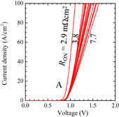
Fig. 4. Forward J–V characteristics of 17 SBDs with 200-µm-diameter Schottky contacts at room temperature. All of them exhibit reasonable turn-on action with low forward voltages and small on-resistances.
Download figure:
Standard image High-resolution image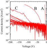
Fig. 5. Reverse J–V characteristics of the same SBDs in Fig. 4. Most of the diodes show relatively small reverse currents with some exceptions (A, B, and C).
Download figure:
Standard image High-resolution image
On the other hand, most of the SBDs did not show breakdown up to −200 V, which is the limit for reverse bias in our measurement system. The typical reverse currents were of reasonable orders (10−5–10−4 A/cm2 at −200 V) considering that the devices were fabricated without dielectric surface passivation. These currents can be further suppressed by passivation or utilizing our recently developed trench MOS structure.13) There are some exceptions (labelled as A, B, and C in Figs. 3 and 5) with leaky behaviour. SBD A behaved almost like a conductor at reverse biases. Together with its forward characteristics, this implies that there was almost no drift layer, that is, the surface of the original wafer was almost exposed after CMP in the position of diode A. For diodes B and C, the breakdown occurring at lower voltages could be attributed to structural imperfections in the epitaxial layer such as surface defects or threading dislocations. The former could be intrinsic or due to mechanical damage24) during CMP. In SBDs fabricated on a  β-Ga2O3 single-crystal substrate, it was indicated that dislocation defects along the [010] direction acted as main paths for leakage current.25) However, there are a few studies on dislocation in (010)- or
  -oriented β-Ga2O3 wafers26,27) but none on dislocations in (001)-oriented ones. Therefore, further studies are required to determine the exact origin of the leakage currents observed here.
In summary, we demonstrated for the first time the growth of thick homoepitaxial layers of β-Ga2O3 on 2-in.-diameter (001) substrates by the HVPE method. An average growth rate of 3–4 µm/h was obtained. Ni SBDs formed on the homoepitaxial wafers after CMP of the HVPE-grown layer surface showed reasonable forward and reverse J–V characteristics. Typical breakdown voltage and on-resistance for SBDs with a drift layer of 5.3 µm thickness and a carrier concentration of 3.4 × 1016 cm−3 were >200 V and 3.8–7.7 mΩ cm2, respectively. In practice, along with efforts in developing advanced device structures, the scalability of the wafer up to larger sizes is indispensable for a material to be applied in real devices. Therefore, the results obtained herein for the 2-in.-diameter homoepitaxial wafers imply an optimistic applicability of β-Ga2O3 at a practical level.