

Abstract
We report (010)-oriented β-Ga2O3 bevel-field-plated mesa Schottky barrier diodes grown by low-pressure chemical vapor deposition (LPCVD) using a solid Ga precursor and O2 and SiCl4 sources. Schottky diodes with good ideality and low reverse leakage were realized on the epitaxial material. Edge termination using beveled field plates yielded a breakdown voltage of −190 V, and maximum vertical electric fields of 4.2 MV/cm in the center and 5.9 MV/cm at the edge were estimated, with extrinsic RON of 3.9 mΩ·cm2 and extracted intrinsic RON of 0.023 mΩ·cm2. The reported results demonstrate the high quality of homoepitaxial LPCVD-grown β-Ga2O3 thin films for vertical power electronics applications, and show that this growth method is promising for future β-Ga2O3 technology.
Export citation and abstract BibTeX RIS
β-Ga2O3 is an ultra-wide bandgap semiconductor with a room-temperature bandgap of 4.5–4.9 eV1,2) and an estimated breakdown field of 6–8 MV/cm.3) Its high breakdown field leads to large theoretical figures of merit for power switching,4) with a lower expected on-resistance (RON)3–5) for a given breakdown voltage (VBR) than those of incumbent wide bandgap materials such as SiC and GaN. The availability of large-area, high-quality native Ga2O3 substrates prepared by scalable and low-cost melt-grown techniques6–10) make Ga2O3-based power devices promising for technological insertion in high-power systems. Lateral devices such as field-effect transistors11–18) and vertical devices including Schottky rectifiers19–25) and trench MOSFETs26–28) have been recently demonstrated by various groups using both β- and α-Ga2O3.29)
Vertical devices are preferred over lateral geometries for high-power applications, but vertical device topologies require an epitaxial growth technology capable of growing thick and low-doped drift layers. Several growth techniques, including molecular beam epitaxy30–32) (MBE), pulsed layer deposition33) (PLD), mist-CVD,29) atmospheric-pressure CVD34) (APCVD), low-pressure CVD35,36) (LPCVD), halide vapor phase epitaxy37) (HVPE), and metal organic chemical vapor deposition38,39) (MOCVD), have been demonstrated for the growth of β-Ga2O3. HVPE with a growth rate of 5 µm/h on (001)37) and LPCVD with a growth rate of ∼2 µm/h on (010) substrates36) are two demonstrated homoepitaxial growth technologies with relatively high growth rates. In addition, LPCVD provides a low-cost solution for growing high-quality epitaxial Ga2O3 with controllable doping40) and high electron mobility compared with other present techniques. Using HVPE, Schottky diodes with planar field-plate termination23) exhibiting breakdown voltage greater than 1 kV have already been demonstrated. However, there are no reports to date on Schottky diodes fabricated using LPCVD-grown β-Ga2O3 films. In this work, we have fabricated Schottky diodes to verify the material quality and investigate device performance in order to demonstrate the viability of LPCVD as a growth technique for vertical power electronic devices. The fabricated diode exhibits a breakdown field (FBR) of 4.2 MV/cm, extrinsic RON of 3.9 mΩ·cm2, and extracted intrinsic RON of 0.023 mΩ·cm2. The extracted FBR is higher than the theoretical FBR values for 4H-SiC (2.2 MV/cm)41) and GaN (3.3 MV/cm).41) The high-performance devices obtained on LPCVD-grown layers demonstrate the potential of this growth method for future β-Ga2O3 technology.
A three-dimensional representation of the fabricated beveled field-plate Schottky diode is shown in Fig. 1(a), along with its cross-sectional schematic in Fig. 1(b). The epitaxial stack consists of ∼2 µm β-Ga2O3 thin film grown by LPCVD on commercially available Sn-doped (010) β-Ga2O3 substrates.43) Growth was carried out in a horizontal furnace with programmable temperature and precise pressure controllers. A growth temperature of 900 °C and a pressure of 4 Torr were used, leading to a nominal growth rate of 2 µm/h. Pregrowth sample preparation involved solvent cleaning using acetone, toluene, and isopropyl alcohol, followed by an N2 blow-dry. Prior to the growth, the samples were annealed in situ at 900 °C for 30 min in O2 ambient. High-purity gallium pellets (Alfa Aesar, 99.99999%) and O2 were used as the source materials and argon (Ar) was used as the carrier gas. Silicon tetrachloride (SiCl4) was used as the n-type dopant source. Atomic force microscopy (AFM) on the sample surface after growth showed a root-mean-square (rms) surface roughness (trms) of 4.86 nm, as seen in Fig. 1(c).

Fig. 1. (a) 3D schematic of the fabricated Schottky barrier diode. (b) 2D cross schematic highlighting the epitaxial stack, the contacts, and field plate. LFP (∼4 µm) is the field-plate overlap and LAB (0.25 µm) is the anode-bevel extension. (c) AFM image for the as-grown β-Ga2O3 film by LPCVD.
Download figure:
Standard image High-resolution imagei-Line stepper lithography was used in the processing of the diodes. The diode fabrication commenced with the deposition of the anode (Pt/Au/Ni) using an e-beam evaporator with Pt as the work function metal. The anode electrode in the devices discussed here is a stripe [Fig. 1(a)] of 50 µm length and 1 µm width designed with rounded corners to avoid breakdown voltage degradation due to the formation of spherical junctions.42) The cathode ohmic contact was deposited on the back of the substrate using e-beam-deposited Ti/Au/Ni. Bevel/trench patterns were formed, which covered the anode metal and extended nominally 0.25 µm from the anode edge on all sides. The device breakdown just after the formation of the anode and cathode was achieved at a depletion width of ∼0.8 µm; hence, the anode-bevel extension (LAB) was chosen as 0.25 µm (<0.8 µm) to leverage the advantages of a bevel design.42) Further details of the device simulation and design are provided later. Subsequently, dry etching to form the trench was carried out in a Plasma-Therm SLR 770 ICP-RIE system using BCl3/Ar gas flow of 35/5 sccm, 30 W RIE, 200 W ICP, and 5 mTorr chamber pressure. In previous studies, dry etching using BCl3 was shown to result in an inclined profile.44) AFM was used to measure the etch depth (t) and the bevel angle (φ) as ∼800 nm and ∼56°, respectively (Fig. 2). Thereafter, 300 nm of SiO2 was deposited conformally by plasma-enhanced CVD (PECVD) at 250 °C as a surface passivation layer. A SiO2 thickness of 300 nm was chosen on the basis of the results of two-dimensional simulations using Silvaco ATLAS to target FBR ∼5 MV/cm. To form the metal field-plate, the oxide layer on top of the anode metal was etched away to form a contact between the anode and the metal plate deposited by conformal sputtering of Ti. Finally, the field plates with a field-plate overlap (LFP) of ∼4 µm were patterned with the remaining metal being etched using dilute hydrochloric acid (HCl) at 65 °C. Figure 3(a) shows the scanning electron microscopy (SEM) images of the diode after field-plate integration where the beveled profile is distinct. Figure 3(b) shows the SEM image for one end of the diode along its length with the rounded pattern designed to avoid sharp corners.

Fig. 2. (a) AFM image for trench analysis. (b) Measured step profile and bevel (slant) angle along the cutline (AA').
Download figure:
Standard image High-resolution image
Fig. 3. SEM images of (a) center portion of the diode after field-plate fabrication and (b) one edge of the diode showing inclined curvature.
Download figure:
Standard image High-resolution imageElectrical characteristics were measured using an Agilent B1500A semiconductor device analyzer. Room-temperature current–voltage (J–V) characteristics of the device are shown in Fig. 4(a). The anode current density vs voltage curves were plotted and compared for the following three structures: (a) after the formation of anode and cathode electrodes and before trench etching, (b) after trench etching and before the deposition of SiO2, and (c) after the final fabrication step. An ideality factor (η) of 1.03 ± 0.02, a high ION/IOFF ratio of ∼1010, and a specific on-resistance (RON) of 3.6 mΩ·cm2 were calculated before trench etching. ION for the diode decreases after BCl3/Ar etching, accompanied by increases in RON to 6.7 mΩ·cm2 and η to 1.1 ± 0.03. We believe that the increase in resistance is related to surface damage that is subsequently repaired during the passivation. The mechanism of this is not understood at present. This is similar to previous reports on BCl3/Ar etching being unfavorable for Schottky diodes.45) With the formation of the field plate, RON decreased to 3.9 mΩ·cm2, and similar characteristics to those before trench etching were obtained, suggesting that the surface damage caused by BCl3/Ar etching was passivated by the SiO2. Figure 4(b) shows the charge profiles before and after trench etching as a function of the depletion width. A doping density (ND) of 2.5 × 1017 cm−3 was obtained from capacitance–voltage (C–V) measurements (the C–V characteristics from which the corresponding charge profiles were extracted are shown in the inset). The measured charge density was similar before and after trench etching, suggesting that while BCl3/Ar etching results in damage of the sidewall surface, it does not cause significant charge depletion. The C–V plot after the formation of the field plate includes contributions from the Ti/SiO2/Ga2O3 (metal oxide semiconductor) sidewall and bond-pad regions, and is therefore not shown here.

Fig. 4. (a) Before trench etching, (b) after trench etching, and (c) field-plate Schottky diode schematics. (d) J–V characteristics of the device at different stages of the diode process with log plot for the device before trench etching in the inset. (e) Charge profile plot along with C–V curves in the inset.
Download figure:
Standard image High-resolution imageFigure 5(a) shows the two-terminal reverse current breakdown characteristics for identical, fresh devices at various stages of the process, with immersion in Fluorinert46) to prevent air breakdown. An anode current compliance of 0.2 A/cm2 (3–4 orders of magnitude lower than ION) is seen to cause destructive breakdown with a breakdown voltage (VBR) of −138 V for diodes before trench etching and −74 V after trench etching. This indicates that the expected enhancement in breakdown voltage using a bevel edge-termination design was not obtained after BCl3/Ar etching. Further analysis is needed to understand this, but one possible reason could be the surface damage caused by BCl3/Ar etching,45) which leads to surface-related leakage. By fabricating the field-plate structure on top of the "after trench" device, VBR was increased from −74 to −190 V. Field-plated Schottky diodes were also found to withstand one order higher current density (>1 A/cm2) before breaking down catastrophically.
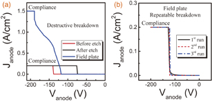
Fig. 5. (a) Two-terminal destructive reverse breakdown characteristics. (b) Nondestructive breakdown for the field-plated device.
Download figure:
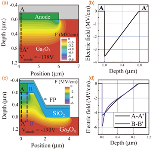
Standard image High-resolution imageThe reverse current seen in the curve after −130 V was deduced to be leakage current through SiO2, which adds to the overall current. Setting a current compliance of 0.2 A/cm2 for the field plates resulted in repeatable breakdown [Fig. 5(b)] with VBR = −129 V. The measured VBR values, Schottky contact barrier height (1.5 eV), and doping density (both extracted from the C–V data) were used to calculate the depletion width (Wdep) and peak electric field (Fmax) using one-dimensional Poisson's equation. Wdep of 0.8 µm, which corresponds to Fmax of 3.5 MV/cm, was estimated for the device before trench etching. Since Wdep of 0.8 µm is less than the epitaxial layer thickness (∼2 µm), this corresponds to non-punch-through breakdown of the devices. Two-dimensional device simulations using Silvaco ATLAS were used to estimate the electric field at the center of the diode, as shown in Fig. 6(b). The foot edge of the anode shows a peak field higher than the theoretical Ga2O3 breakdown field (8 MV/cm), similar to a previous report.23) The corresponding Wdep and Fmax values for the device after trench etching decreased to 0.65 µm and 2.4 MV/cm, respectively. With the field plate, Fmax of 3.4 MV/cm for repeatable breakdown and 4.2 MV/cm for destructive breakdown were calculated (i.e., Fmax increased from 2.4 MV/cm after trench etching to 4.2 MV/cm after field-plate insertion). 2D Silvaco simulations for destructive breakdown on the field plate were seen to match the calculated 4.2 MV/cm field at the center of the diode with the peak field of 5.9 MV/cm at the corner. The calculated values of Wdep and Fmax are tabulated in Table I. The last column in the table lists the intrinsic RON values for all ND and Wdep values estimated using the equation

where q = 1.6 × 10⁻¹⁹ C is the elementary electric charge and μ is the mobility (∼100 cm2 V−1 s−1, estimated from the Hall measurement of in-plane mobility). As expected for a back contact, the measured device resistance is dominated by the extrinsic resistance of the substrate.
Fig. 6. (a) 2D Silvaco ATLAS simulations to highlight vertical electric field (F) contour map in Ga2O3 (a) before trench etching and (c) after field-plate (FP) insertion. (b) and (d) Measured field magnitudes along the cutlines.
Download figure:
Standard image High-resolution image
Table I. All the experimental VBR values and corresponding calculated Wdep, Fmax, and RON.
| Diode structure | VBR (V) | Wdep (µm) | Fmax (MV/cm) | RON (mΩ·cm2) | |
|---|---|---|---|---|---|
| Before trench | −138 | 0.80 | 3.5 | 0.019 | |
| After trench | −74 | 0.65 | 2.4 | 0.020 | |
| Field plate | BD1 | −190 | 0.92 | 4.2 | 0.023 |
| BD2 | −129 | 0.76 | 3.4 | 0.019 |
BD1: Destructive breakdown
BD2: Repeatable breakdown for the field-plated diodes
In summary, we demonstrated a field-plate bevel mesa Schottky diode using LPCVD-grown β-Ga2O3 thin film. A high breakdown field of 4.2 MV/cm, extrinsic RON of 3.9 mΩ·cm2, and intrinsic RON of 0.023 mΩ·cm2 were estimated for the devices, indicating the high quality of the LPCVD-grown layers. Device performance degradation due to BCl3/Ar was mitigated by SiO2 passivation. Future developments in epitaxial growth for lower background doping and field management will enable β-Ga2O3 power devices with lower conduction and switching losses. The reported work shows the promise of LPCVD β-Ga2O3 for low-cost high-power devices.
Acknowledgments
We acknowledge funding from the Department of Defense, Defense Threat Reduction Agency (Grant HDTRA11710034), National Science Foundation (DMR-1755479), ONR EXEDE MURI program, and the OSU Institute for Materials Research Seed Program. We thank the Air Force Research Laboratory (D. Dorsey, G. Jessen, and K. Chabak) for support. The content of the information does not necessarily reflect the position or the policy of the federal government, and no official endorsement should be inferred.