
Abstract
We report on extremely low off-state leakage current in AlGaN/GaN-on-silicon metal–insulator–semiconductor high-electron-mobility transistors (MISHEMTs) up to a high blocking voltage. Remarkably low off-state gate and drain leakage currents below 1 µA/mm up to 3 kV have been achieved owing to the use of a thick in situ SiN gate dielectric under the gate, and a local Si substrate removal technique combined with a cost effective 15-µm-thick AlN dielectric layer followed by a Cu deposition. This result establishes a manufacturable state-of-the-art high-voltage GaN-on-silicon power transistors while maintaining a low specific on-resistance of approximately 10 mΩ·cm2.
Export citation and abstract BibTeX RIS

Content from this work may be used under the terms of the Creative Commons Attribution 4.0 license. Any further distribution of this work must maintain attribution to the author(s) and the title of the work, journal citation and DOI.
Corrections were made to this article on 25 May 2018. The article was made open access.
For future efficient and low-cost power electronics, GaN high-electron-mobility transistors (HEMTs) on silicon (Si) substrate are highly promising owing to their superior intrinsic properties such as large bandgap, high breakdown field strength, and high electron saturation velocity.1–9) However, GaN-on-Si transistors suffer from poor critical electrical field strength of the Si substrate together with a parasitic conduction at the buffer/substrate interface leading to device breakdown.10–12) Therefore, the highest reported three-terminal breakdown voltage (VBD) values for GaN-on-Si HEMTs defined at an off-state leakage current of 1 µA/mm are still below 1.5 kV,13) which is basically limited by the Si substrate and the associated material quality.14–21)
To suppress the parasitic conduction phenomenon, a local Si substrate removal (LSR) was proposed in 2010.22,23) The Si substrate removal around the drain electrode enabled the electrical isolation of the gate and source from the drain across the buffer layer/Si interface, leading to an enhanced blocking voltage of the GaN-on-Si HEMT above 2 kV.24) Using this approach, our group reported GaN-based transistors with a significantly improved blocking voltage of 3 kV,25) but still with a high leakage current that is not compatible with high-power applications.
In this paper, we report for the first time GaN-on-Si metal–insulator–semiconductor HEMTs (MISHEMTs) with LSR under the entire device followed by a backside deposition of the ultra-wide bandgap AlN material. The use of an in situ SiN gate dielectric under the gate and the LSR technique combined with 15-µm-thick AlN layer enabled the state-of-the-art GaN-based HEMTs with remarkably low off-state leakage current (<1 µA/mm) up to 3 kV.
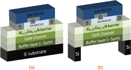
The AlGaN/GaN/AlGaN double heterostructures were grown using metalorganic chemical vapor deposition (MOCVD) on a 6-in. Si(111) substrate. The HEMT structure consists of an AlN nucleation layer followed by AlGaN-graded transition layers and an Al0.08Ga0.92N buffer layer. The 5 µm total buffer thickness was followed by a 150-nm GaN channel, a 20-nm Al0.25Ga0.75N barrier layer and a 50-nm in situ Si3N4 cap layer [Fig. 1(a)]. Hall effect measurements revealed an electron sheet concentration of 8.9 × 1012 cm−2 with a mobility of 2190 cm2·V−1·s−1 and a sheet resistance RSH = 319 Ω/□ at room temperature with a high uniformity of less than 4% across the wafer. Ohmic contacts were formed directly on top of the AlGaN barrier by alloying the Ti/Al/Ni/Au stack at 875 °C using rapid thermal annealing. Device isolation was achieved by N2 implantation. The metal–insulator–semiconductor (MIS) gate structure was employed by depositing the Ni/Au metal stack on the in situ Si3N4 cap layer (30-nm-thick SiN left under the gate) without any additional field plate. A 200-nm-thick SiN film was deposited using plasma-enhanced chemical vapor deposition (PECVD) as extra passivation. Once the front-side processing was completed, the Si substrate was locally etched up to the AlN nucleation layer around the entire device (50 µm away from the sidewalls), as shown in Fig. 1(b). It is noteworthy that our mask design consists of devices with and without LSR patterns, which eliminates any processing or epi variations during the device characterization [Fig. 2(a)]. Figure 2(b) depicts a backside view of a crack-free 20 × 500 µm2 GaN-based MISHEMT after the LSR technique.
Download figure:
Standard image High-resolution image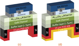
Fig. 1. Schematic cross-section of AlGaN/GaN MISHEMT after the (a) front side process, (b) LSR technique, (c) 15-µm-thick PVD AlN deposition, and (d) 2-µm Cu deposition on the backside.
Download figure:
Standard image High-resolution image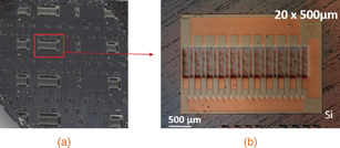
Fig. 2. Optical backside image of (a) the wafer with and without LSR removal patterns, (b) 20 × 500 µm2 GaN-based MISHEMT after LSR.
Download figure:
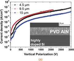
Standard image High-resolution imageSubsequently, a 15-µm-thick AlN was deposited on the backside by physical vapor deposition (PVD) at 300 °C by Kyma Technologies. Figure 3(a) reveals the cross-sectional scanning electron microscopy (SEM) image of the 15-µm-thick conformal AlN film. To evaluate the corresponding breakdown voltage characteristics, several thicknesses have been deposited on a highly doped Si. The PVD AlN film delivered a high breakdown field above 4 MV/cm despite the low temperature deposition, and offers a cost-effective manufacturing technology scalable up to 8 inches, considering that the LSR approach is also applicable in large-diameter wafers. In addition, Fig. 3(b) shows the vertical leakage current measurements conducted on isolated transmission line method (TLM) patterns on structures A and B. Structures A and B correspond to the AlGaN/GaN epitaxial designs without and with LSR/backside AlN deposition, respectively. The removal of the Si substrate combined with the backside deposition of a 15-µm-thick AlN layer enabled a remarkable increase in the vertical breakdown from 850 V to 2.6 kV, confirming the suppression of substrate conduction and the effectiveness of the dielectric film.
Download figure:
Standard image High-resolution image
Fig. 3. Vertical leakage characteristics of (a) AlN layers deposited under the same conditions as a function of thickness on highly doped Si, and (b) AlGaN/GaN epitaxial structures A and B, without and with LSR/backside AlN deposition, respectively. Inset: Cross-sectional SEM image of 15-µm-thick AlN film.
Download figure:
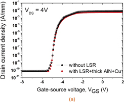
Standard image High-resolution imageElectrical characterizations were carried out on devices with gate width/length = 50 µm/2 µm and a gate-to-drain spacing (LGD) that varied from 2 to 40 µm with and without LSR/backside AlN and Cu deposition on the same wafer. The DC transfer and ID–VD characteristics of the AlGaN/GaN MISHEMTs with an LGD of 40 µm are shown in Fig. 4. The maximum current density at VGS = +1 V decreased by approximately 30% from 8.8 to 6.3 mA/mm after the Si substrate removal under the active region due to self-heating. The origin of the self-heating subsequent to substrate removal is the degradation of the thermal dissipation in air, resulting in an increase in the channel temperature, which decreases the electron mobility and thus causes a reduction in the drain current. Indeed, the devices with LSR have been recently reported to have lower thermal conductivities than those without LSR by the Raman thermometry technique.26) However, a significant recovery of the maximum current density (approximately 85%), with respect to the devices without LSR, occurs after the highly thermally conductive Cu deposition, which in turn enables the strong reduction in self-heating [Fig. 4(b)]. The static specific on-resistance (RON-STATIC) values were extracted to be 13.1 and 13.2 mΩ/cm2 for devices with LGD = 40 µm, without and with LSR/thick AlN and Cu, respectively. The active area of the devices with LGD = 40 µm was calculated to be 2.6 × 10⁻⁵ cm2 by considering a 5 µm transfer length for each ohmic contact (i.e., source and drain).
Download figure:
Standard image High-resolution image
Fig. 4. (a) DC transfer and (b) ID–VD characteristics of GaN-based MISHEMTs with LGD of 40 µm with and without LSR/backside AlN and Cu deposition.
Download figure:
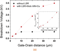
Standard image High-resolution imageThree-terminal VBD measurements were conducted on various transistor designs from 2 to 40 µm at VGS = −8 V with a floating substrate using a Fluorinert solution. VBD was defined as the drain–source voltage (VDS) at which the drain current density (ID) reaches 1 µA/mm. The specific on-resistances and breakdown voltages without and with LSR/thick AlN and Cu for each design are represented in Fig. 5(a). For devices without LSR, VBD saturated at approximately 600 V for LGD larger than 10 µm resulting from the parasitic substrate conduction between the metal contacts and the Si substrate, regardless of the device geometry. The device breakdown occurs at the AlN/Si interface because of the lower breakdown field of Si compared to the III–nitride layers (EAlN = 11.7 MV/cm and ESi = 0.3 MV/cm).10,11) On the other hand, for devices with LSR/thick AlN and Cu, the substrate leakage contribution is suppressed and VBD further increased with the gate-to-drain distance while still delivering low specific on-resistances.
Download figure:
Standard image High-resolution image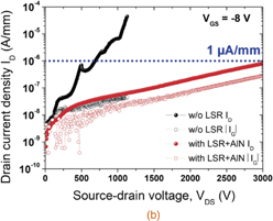
Fig. 5. (a) Evolution of LGD-dependent device breakdown and specific on-resistance (inset) of AlGaN/GaN HEMTs with and without LSR/thick AlN/Cu by defining blocking voltage at ID = 1 µA/mm, and (b) off-state leakage current characteristics of AlGaN/GaN MISHEMTs with and without LSR/thick AlN deposition.
Download figure:
Standard image High-resolution imageThe three-terminal off-state leakage characteristics of the AlGaN/GaN MISHEMTs with and without LSR/thick AlN and Cu are plotted as a function of VDS for the largest design, i.e., LGD = 40 µm in Fig. 5(b). The devices without LSR demonstrated an exponential increase in the leakage current at low VDS bias reaching the 1 µA/mm limit at approximately 600 V owing to the parasitic conduction through the buffer/Si substrate. For devices with LSR/thick AlN and Cu, the drain leakage current density was reduced by approximately two orders of magnitude from 600 V to 3 kV, confirming the suppression of the substrate's conductive-path contribution. It is noteworthy that the off-state gate leakage (IG) currents of both AlGaN/GaN MISHEMT designs, with and without LSR are below 1 µA/mm until the device breaks down owing to the gate dielectric under the gate. Therefore, despite common perception, the drain leakage current flowing through the buffer layers is not especially due to the bulk defects/traps but is more confined at the AlN nucleation layer/Si substrate interface.
Figure 6 shows a benchmark of the GaN-on-Si HEMTs blocking voltage defined at an off-state leakage current of 1 µA/mm.27–30) The translated specific RON of 13 mΩ·cm2 combined with a blocking breakdown voltage of 3 kV, for devices with LGD = 40 µm sets the state-of-the-art device. These results pave the way for higher-voltage-operation GaN-on-Si power devices.

Fig. 6. Benchmark of GaN-on-Si HEMTs with blocking voltage defined at an off-state leakage current of 1 µA/mm.
Download figure:
Standard image High-resolution image
We demonstrated for the first time GaN-on-Si MISHEMTs with local Si substrate removal under the entire device followed by a low-cost backside deposition of a thick ultra-wide bandgap AlN film. Using an MIS gate structure and the LSR technique combined with a 15-µm-thick AlN layer resulted in state-of-the-art GaN-based HEMTs with remarkably low off-state leakage current (<1 µA/mm) beyond 3 kV. The comparison of these devices without LSR proves that the drain leakage current flows at the AlN nucleation layer/Si substrate interface. Furthermore, the significant recovery of the maximum current density after the backside Cu deposition enabled the reduction in self-heating. This work shows that this emerging type of devices could be useful for cost-effective applications requiring breakdown voltages above 3 kV.
Acknowledgments
This work is supported by the French RENATECH network and the ANR project DESTINEE (ANR-16-CE05-0022). This project has received funding from the European Union's Horizon 2020 research and innovation program under grant agreement No. 720527 (Inrel–NPower). The authors would also like to gratefully acknowledge the company EpiGaN for the high material-quality delivery as well as the company Kyma for the thick PVD AlN deposition.