Abstract
Results of GaN growth from gallium solution under high nitrogen pressure are presented. Basic of the high nitrogen pressure solution (HNPS) growth method is described. A new approach of seeded growth, multi-feed seed (MFS) configuration, is demonstrated. The use of two kinds of seeds: free-standing hydride vapor phase epitaxy GaN (HVPE-GaN) obtained from metal organic chemical vapor deposition (MOCVD)-GaN/sapphire templates and free-standing HVPE-GaN obtained from the ammonothermally grown GaN crystals, is shown. Depending on the seeds' structural quality, the differences in the structural properties of pressure grown material are demonstrated and analyzed. The role and influence of impurities, like oxygen and magnesium, on GaN crystals grown from gallium solution in the MFS configuration is presented. The properties of differently doped GaN crystals are discussed. An application of the pressure grown GaN crystals as substrates for electronic and optoelectronic devices is reported.
Export citation and abstract BibTeX RIS
1. Introduction
Although gallium nitride based devices, such as light emitting diodes (LEDs) or high electron mobility transistors (HEMTs), are mainly built on foreign substrates (sapphire, silicon and silicon carbide), the nitride community is still looking for GaN substrates in order to replace the foreign ones. In particular, one class of devices, namely laser diodes (LDs), requires native GaN substrates. Today, the UV, blue, and green LDs are exclusively built on the GaN foundation. Many people believe lasers to constitute the next generation of lighting (after LEDs), even for general applications (projectors, displays, automotive lighting, etc.). First of all, the LDs are more efficient and offer natural white light. Secondly, the LDs' advantage is that they can be packed more densely on a chip than the LEDs. Working on its new car model, the BMW applies blue laser diodes, knowing that the blue LD is 1000 times as bright as the LED, though uses just two-thirds of the energy.1) Considering that the LDs' market will keep developing faster, having and using the GaN substrates seems to be necessary. They have to be at least of 2-in. diameter, with relatively high structural quality (structurally flat with low threading dislocation density), and a free carrier concentration higher than 2 × 1018 cm−3. This last feature provides a possibility of making appropriate electric contacts to the epitaxial laser diodes structures. On the other hand, people are dreaming about new high power electronic devices based on native GaN. For this application the GaN substrates should be at least of 4 in. diameter and available at different levels of carrier concentration from n-type to semi-insulating type.
It is not easy to prepare the GaN substrates. The gallium nitride compound melts at an extremely high temperature of 2493 K. The nitrogen pressure necessary for congruent melting of GaN is 6 GPa.2) Thus, today it is impossible to crystallize GaN just from the melt using the Czochralski or Bridgman methods. This compound should be grown by other techniques requiring lower pressure and temperatures. Crystallization from gas phase, solution, or any combinations thereof must be included.
Today, due to a relatively high growth rate (>100 µm/h) and a possibility to crystallize high-purity material, hydride vapor phase epitaxy (HVPE) is the most common approach for manufacturing GaN substrates.3–9) This involves crystallization from the vapor phase at ambient pressure. GaN is deposited on a foreign substrate through the reaction of ammonia with gallium chloride at temperatures of about 1300 K. Etching and self lift-off techniques can be used to remove the nitride film from the foreign substrates' typically sapphire or gallium arsenide, and yield a large-diameter, free-standing 2, 4, or 6 in. GaN. Deposition on a foreign foundation enables the growth of large diameter GaN crystals, but these suffer from lattice bowing. This stems from significant differences between the lattice constant and thermal expansion coefficient of the foreign substrate and the nitride film. When GaN is grown by HVPE on sapphire, the bowing radii of crystallographic planes for 2 in. substrates is always below 10 m. This is the reason why free standing HVPE-GaN crystals cannot be commonly used as seeds for further HVPE growth. There is no advantage of crystallizing on a "bent seed" without any possibility of improving its crystallographic quality. This is also the reason why bigger than 2 in. free standing HVPE-GaN substrates are not mass-produced. They are too bent (from crystallographic point of view) and, therefore not suitable for processing in the production of electronic and optoelectronic devices. On the other hand, it is not possible to misorient HVPE-GaN substrates uniformly, which is important for epitaxy and doping of AlInGaN structures. The epi layer's quality, as well as incorporation of dopants, depend on the miscut degree of the substrate.10–12)
Recently, it has been shown how to overcome these issues and grow crystallographically flat, free-standing HVPE-GaN by using structurally perfect ammonothermally grown GaN crystals as seeds13) and/or applying free-standing HVPE-GaN as seeds for high nitrogen pressure solution growth. It should be noted, herein, that growth from solution is the second possibility (beside the HVPE) to grow gallium nitride crystals. For GaN crystallized from the solution, the maximum size of the free standing GaN substrate obtained in laboratories today is 3 in. (by sodium-flux method14)), but only 1 in. substrates are commercially available.15) Generally, crystallization from the solution can be divided into crystallization from solution in supercritical ammonia (ammonothermal method) and from solution in gallium (high nitrogen pressure solution growth method) or gallium–sodium mixtures (sodium flux method). Each of these technologies requires higher than atmospheric pressure. The role of the pressure, its value, as well as its medium (nitrogen or ammonia) are definitely different for each of the growth method. In the ammonothermal growth high pressure allows to obtain supercritical ammonia, which leads to sufficient solubility of GaN in the supercritical solution. Ammonothermal approach is analogous to hydrothermal crystallization of quartz, however supercritical ammonia is used in place of water. Herein, supersaturation is created by the presence of temperature gradient. Thus, the mass transport is governed by convection.16–18) In turn, in the sodium flux method the high pressure of nitrogen ensures the supersaturation in the flux, because its value is higher than the equilibrium one for considered phases of the flux.19,20) The growth proceeds at constant temperature. The mass transport is governed by convection caused by mechanical stirring of the flux. For the growth from gallium solution, the high nitrogen pressure allows to increase the thermodynamic stability range of GaN. Therefore, crystallization at relatively high temperatures (∼1800 K) becomes possible. In this case, the supersaturation is created by the presence of temperature gradient in the solution, and the mass transport (as in the ammonothermal method) is governed by convection.
In this paper the high nitrogen pressure solution (HNPS) growth method is described. A basic of this method is demonstrated. The paper is focused on seeded crystallization under pressure. Relatively new approach of seeded growth, a multi-feed seed (MFS) configuration, is analyzed in detail. Two kinds of seeds are used: free-standing HVPE-GaN obtained from metal organic chemical vapor deposition (MOCVD)-GaN/sapphire template and HVPE-GaN crystallized and then sliced from ammonothermally grown GaN. The influence of structural quality of seeds on structural quality of the new, pressure grown material is demonstrated. Results of crystallization of strongly n-type and semi-insulating material are presented. Properties of differently doped HNPS-GaN crystals are also shown. An application of the pressure grown GaN crystals as substrates for laser diodes and high mobility electronic structures is briefly reported.
2. Experimental methods
The HNPS growth method is a temperature gradient method based on a direct reaction between liquid gallium (Ga) and gaseous nitrogen (N2) at a high temperature (up to 1800 K) and a high nitrogen pressure (up to 1 GPa). Nitrogen molecules dissociate on gallium surface and dissolve in the metal. Therefore, the crystals are grown from the solution of atomic nitrogen (N) in liquid gallium. Supersaturation, the driving force of the crystallization process, is created by the application of temperature gradient along the liquid gallium. Due to this gradient, the atomic nitrogen is transported from the hot end of the solution to the cooler part. It was shown21–23) that the convection mechanism plays a dominant role in the transport phenomenon and that nitrogen in the solution is uniformly distributed only due to the convection flow. Since the excess nitrogen concentration related to the equilibrium value at a given temperature exists at the cold part of the liquid metal, the solution is supersaturated there. Hence, the GaN crystal growth takes place only in this relatively cold zone. The gallium nitride crystals can be grown spontaneously from the walls of the crucible, having a habit of hexagonal platelets or needles.24,25) They are distributed randomly in the supersaturated zone of the solution. For a seeded crystallization, GaN or foreign seeds have to be immersed in the gallium at supersaturated zone of the solution.26,27) The schematic illustrations of the spontaneous and seeded growth by the HNPS method are presented in Figs. 1(a) and 1(b), respectively.

Fig. 1. Schematic illustration of the crystallization process in a temperature gradient by the HNPS method: (a) spontaneous crystallization; (b) seeded growth; three stages of the HNPS method: dissociative adsorption of nitrogen on liquid metal surface; dissolution and transport of nitrogen atoms from a hot end of the solution to the cooler one; crystallization process; are marked.
Download figure:
Standard image High-resolution imageTypical crystal growth experiment is when the metal (Ga) placed in the crucible (graphite or boron nitride) is heated in the furnace inside the high pressure reactor with a constant rate to given axial and/or radial temperature profiles.28) Then, the system is annealed at these conditions under high nitrogen pressure (1 GPa or less) for 100–500 h. After that, the furnace is cooled down at a constant rate, the system is decompressed, and the metal with GaN crystals inside is removed. The charge from the crucible is etched with boiling HNO3/HCl acid solution to extract the crystals. Vertically positioned technological gas pressure chambers (reactors) of internal diameters up to 10 cm, allowing crucibles with the working volume up to 150 cm3, are used.28) The multizone cylindrical graphite furnaces, capable of reaching maximum temperature of 2073 K, are placed inside the gas pressure reactors. To register the temperature during the crystal growth experiments, PtRh6%–PtRh30% thermocouples are used. They are arranged along the furnace and coupled with the input power control electronic systems. The pressure is measured by manganine gauges positioned in the low temperature zone of the reactors. The pressure and temperature are stabilized with an accuracy of 1 MPa and 0.1 K, respectively. One of the typical experimental systems for crystal growth of GaN at high nitrogen pressure is shown in Fig. 2.
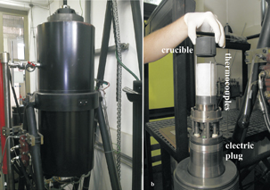
Fig. 2. Experimental system for crystal growth of GaN at high nitrogen pressure: (a) high pressure chamber; (b) crucible with a set of thermocouples and an electric plug.
Download figure:
Standard image High-resolution imageDuring the crystallization process, the pressure and the temperature in the whole gallium sample correspond to the nitride stability range. Thus, the highest measured temperature is lower than the equilibrium temperature for a given nitrogen pressure at three phase Ga–N2–GaN equilibrium conditions. These conditions were determined by Karpinski et al.29) by a direct synthesis and decomposition experiments performed by both: gas-pressure technique (for pressures up to 2 GPa) and high-pressure anvil technique (up to 7 GPa). The N solubility data resulting from the annealing of Ga in N2 atmosphere at the three-phase Ga–N2–GaN equilibrium conditions for the temperature range from 1573 to 1850 K were determined by Grzegory et al.30,31) In applied temperature range, the nitrogen concentrations in the solution are not very high, always below 1 at. %.
Recently, the MFS configuration in the HNPS growth method has been proposed and developed.32–37) This configuration has been based on the conversion of free-standing HVPE-GaN crystals to free-standing, pressure grown HNPS-GaN of a much higher quality than the seeds. The great strength of this approach is that it yields several GaN crystals from one run — what's more, the crystals satisfy all the criteria for being substrates. Production of this material begins by positioning several (0001) or  -oriented HVPE-GaN seeds in a vertical stack, separated by liquid gallium or liquid gallium doped with magnesium, respectively (see Fig. 3). The lowest seed is placed above the bottom of the crucible and the distance between individual seeds can be varied. Under nitrogen pressures of typically 1 GPa and at temperatures of the level of 1593–1773 K an axial temperature gradient (from 5 to 30 K/cm) is applied along the crucible, leading to an overgrowth of seeds on their upper surface and their dissolution from the opposite side. Due to the dissolution process atomic nitrogen is supplied into the metal solution and is transported to the underlying crystal. In other words, each seed is overgrown and dissolved at the same time, but at slightly different temperatures, varying by approximately a few degrees. Therefore, they are feeds and seeds at the same time, and the liquid gallium discs (sometimes doped by magnesium) play the role of traveling zones.
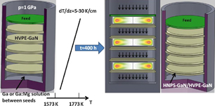
Fig. 3. Scheme of the MFS configuration; the free standing HVPE-GaN substrates are positioned vertically; liquid gallium discs (in some cases doped with magnesium) are between them; due to temperature gradient applied the HVPE-GaN crystals are dissolved in liquid gallium at their bottom sides, supplying atomic nitrogen to the solution; nitrogen is transported in the liquid gallium by convection and/or diffusion to the underlying seed where the crystallization takes place.
Download figure:
Standard image High-resolution imageThe HVPE-GaN crystals, seeds for the HNPS-MFS growth, are prepared in a homemade, horizontal, quartz HVPE reactor. Two-inch and up to 1-mm-thick free standing (FS) HVPE-GaN crystals are obtained using MOCVD-GaN/sapphire templates.38–40) The typical 2-in. FS HVPE-GaN is shown in Fig. 4(a). On the other hand, FS HVPE-GaN can be also obtained by using ammonothermally grown GaN (as seed).13,41,42) One-inch, smooth GaN layers up to 2-mm-thick (crystallized with a stable growth rate of 240 µm/h) and of an excellent crystalline quality, without cracks, and with low threading dislocation density (5 × 104 cm−2) are grown and then sliced from the ammono-GaN seed wafers [see Figs. 4(b) and 4(c), respectively]. The (0001) and  surfaces of all FS HVPE-GaN crystals are prepared to the epi-ready state by a combination of mechanical and mechano-chemical polishing. The typical properties of the FS HVPE-GaN crystals used as seeds for the HNPS-MFS crystallization runs are presented in Table I. It should be noted that from the structural properties point of view, FS HVPE-GaN obtained from ammono-GaN is of a much higher quality than this obtained from MOCVD-GaN/sapphire template.42)

Fig. 4. (a) Typical FS HVPE-GaN crystallized on MOCVD-GaN/sapphire template; (b) HVPE-GaN grown on ammono-GaN seed (as grown crystal); (c) FS HVPE-GaN sliced from the ammono-GaN seed after mechanical polishing; grid 1 mm.
Download figure:
Standard image High-resolution imageTable I. Typical properties of the HVPE-GaN crystallized in IHHP PAS and TopGaN Ltd.
| From MOCVD-GaN/sapphire template | From ammono-GaN seed | |
|---|---|---|
| Free carrier concentration (Hall method) (cm−3) | 2 × 10¹⁶–2 × 10¹⁷ | 2 × 10¹⁶–2 × 10¹⁷ |
| Mobility (Hall method) (cm2·V−1·s−1) | 800–1100 | 800–1100 |
| Etch pits density (cm−2) | 2 × 10⁶–107 | 5 × 10⁴ |
| X-ray (002) reflexion FWHM (beam size 1 × 10 mm2) (arcsec) | 200–500 | 20–100 |
| Absolute value of bowing radius (X-ray measurements) (m) | 1–5 | 20–100 |
3. Results and discussion
3.1. Results
3.1.1. Crystallization without intentional doping
The HNPS crystallization in gallium without intentional doping always leads to n-type HNPS-GaN crystals (free carrier concentration n > 1019 cm−3 24)). As mentioned above, the dominating morphological form of GaN crystals grown in a spontaneous way is a hexagonal platelet.24,25) At higher supersaturation hollowed from inside needles can be obtained.25,28) The main disadvantages of spontaneous crystallization by the HNPS method are: small size and poor reproducibility of the size, and also distribution of GaN crystals in the crucible. A better control of the last two parameters was achieved by growth with seed crystals introduced intentionally into the solution. As was described above, an MFS configuration is generally applied today.
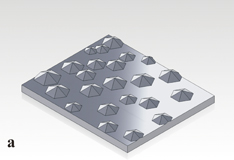
Stable and macroscopically flat crystals are grown in the configuration presented in Fig. 3. Three types of morphology are noted: hillocks, hillocks and macrosteps (mixed) and macrosteps. They are all presented in Fig. 5. The presence of these three growth modes depends on the temperature gradient applied. For the smallest temperature gradient (∼5 K/cm) the hillock growth mode is observed [see Fig. 5(a)]. In this case the growth rate is not higher than 1 µm/h. For a bigger temperature gradient ( 5 K/cm) the mixed growth mode appears. The macrosteps coexist with hillocks on the growing crystal surface [see Fig. 5(b)]. Then the average growth rate reaches 2 µm/h. For bigger still temperature gradient the hillocks disappear and only macrosteps are detected [see Fig. 5(c)], while the growth rate attains even 5 µm/h. In this case some voids and gallium inclusions are observed in the new grown material.

Download figure:
Standard image High-resolution image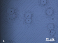
Download figure:
Standard image High-resolution image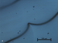
Fig. 5. Three types of morphology of the HNPS-MFS-GaN crystals: (a) hillocks; (b) hillocks and macrosteps; (c) macrosteps with flounces; this is a favorable mode for formation of voids and inclusions of solvent in the HNPS-MFS-GaN.
Download figure:
Standard image High-resolution imageThe total average etch pit density for the examined HNPS-MFS-GaN depends on the quality of the seeds used. For the FS HVPE-GaN obtained from the MOCVD-GaN/sapphire template it is always of the order of 106 cm−2. For the FS HVPE-GaN obtained from the ammono-GaN crystal it is of the order of 105 cm−2, thus only two times more than for the seed used (see Table I). The deposition of the HNPS-MFS-GaN layers and dissolution of HVPE-GaN can improve the structural quality of the obtained crystals.33,35) The X-ray rocking curves are narrower and the lattice bowing radii increase. For FS HVPE-GaN obtained from the MOCVD-GaN/sapphire template and then used in the HNPS-MFS growth method as seed, the absolute value of the bowing radius can increase from 2 to 20 m. For FS HVPE-GaN obtained from the ammono-GaN crystal the absolute value of the bowing radius does not change, remaining the same as that of the seed.
The free carrier concentration in HNPS-MFS-GaN is always higher than 1019 cm−3 and its value depends on the growth temperature. The dependence between the free carrier concentration in the crystals and the growth temperature is presented in Fig. 6(a). With the increase of the growth temperature from 1593 to 1723 K, the carrier concentration in HNPS-MFS-GaN increases. Then, for higher temperature (over 1723 K) it is saturated reaching a constant value of the order of 5 × 1019 cm−3. The secondary ion mass spectrometry (SIMS) analysis of oxygen impurity in the HNPS-MFS-GaN crystals showed that for a given growth temperature the carrier concentration was equal to the concentration of oxygen. Figures 6(b) and 6(c) represent two SIMS spectra for crystals grown in two absolutely different temperatures: 1653 and 1703 K. The difference in oxygen concentration is well visible. Lower concentration is noted for lower growth temperature.

Download figure:
Standard image High-resolution image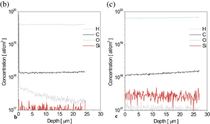
Fig. 6. (a) Free carrier concentration in the function of the growth temperature; up to 1713 K it increases, then, it reaches a constant value of approximately 5 × 1019 cm−3; (b) SIMS spectrum for the HNPS-MFS-GaN crystal grown at 1653 K (lower oxygen concentration); (c) SIMS spectrum for the HNPS-MFS-GaN crystal grown at 1703 K (higher oxygen concentration).
Download figure:
Standard image High-resolution imageAfter a growth run (typically 400 h), the crystals are cut by a drill pipe to round forms of a 16 mm, 20 mm, 1 in., or 1.5 in. diameter following which their (0001) surface is mechanically and mechanochemically polished to the epi-ready state. A scheme of this procedure is shown in Fig. 7. The pinholes visible in the material [see Fig. 7(a)] are always situated at the bottom (nitrogen surface) of the HVPE-GaN seed. No pinholes are observed in the pressure grown material [on its (0001) surface].
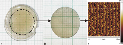
Fig. 7. Scheme of preparing the HNPS-MFS-GaN substrates: (a) as grown crystal; grid 1 mm; (b) cut (by a drill pipe) round form of the HNPS-MFS-GaN crystal; both surfaces were polished by mechanical way; grid 1 mm; (c) part of the epi-ready (0001) surface of HNPS-MFS-GaN after mechanochemical polishing; steps are visible; (RMS = 0.1 nm).
Download figure:
Standard image High-resolution imageThe laser diodes made on HNPS-MFS-GaN substrates (by MOVPE technology) emitted at 390 to 420 nm, had a typical threshold voltage of 4.5 V at 2.5 kA/cm2 and a lifetime of up to 5000 h.43) The HNPS-MFS-GaN crystals were also used for preparing undulated substrates (with locally controlled miscut).44) Laser diodes made on them emitted from 400 to 410 nm at threshold voltage of 5.5 V and 4 kA/cm2. The substrates are called plasmonic substrates due to their extremely high free carrier concentration. Two typical plasmonic GaN substrates are presented in Fig. 8. The plasmonic GaN has an advantage of increasing the refractive index contrast between substrate and epitaxial laser diode structure suppressing optical mode leakage into the substrate and optimizing the optical mode in the active region. This approach is superior than the use of a conventional GaN substrate (with the free electron concentration of the order of 5 × 1018 cm−3 or lower) and adding a thick AlGaN layer or an AlGaN super lattice beneath the active region to prevent light propagating from there into the substrate. Going down this more common route, the strain increases in the epi-structure, leading to macroscopic bowing, cracking and the creation of misfit dislocations.45,46)
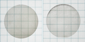
Fig. 8. Typical plasmonic GaN substrates (grid 1 mm).
Download figure:
Standard image High-resolution image3.1.2. Semi-insulating HNPS-MFS-GaN:Mg crystals
For HNPS-MFS-GaN crystallization in the solution of Ga:Mg (up to 1 at. % of Mg) the macroscopically stable growth mode is always observed on the  HVPE-GaN surface. The typical morphology is the macrosteps propagation. For two temperature gradients applied: 10 and 20 K/cm, the growth rate varies from 1 to 2 µm/h. Neither different morphologies (different growth modes), nor gallium inclusions, nor voids in the material are observed. Some objects similar to triangles are often found in the crystallized material.36) The EDS analysis showed that they are MgO crystals. If MgO crystals are not epitaxially overgrown by GaN, they are removed from GaN during mechanical and mechanochemical polishing, forming big pits in the material. The average etch pit density for the examined HNPS-MFS-GaN:Mg depends on quality of the seeds used. For the FS HVPE-GaN obtained from the MOCVD-GaN/sapphire template it is of the order of 5 × 10⁶–107 cm−2. For the FS HVPE-GaN obtained from the Ammono-GaN crystal it is not higher than 5 × 105 cm−2. The bowing radii of the HNPS-MFS-GaN:Mg crystals do not change significantly comparing to the HVPE-GaN seeds (see Table I).
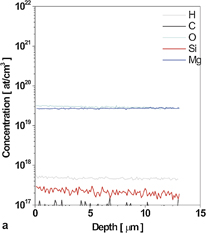
The SIMS analysis shows that the magnesium concentration in the crystals is strictly the same as the oxygen concentration [see Fig. 9(a)]. Figure 9(b) shows resistivity of the HNPS-MFS-GaN:Mg in the function of temperature. It can be clearly seen that this material is definitely semi-insulating. Additionally, its electrical properties are very stable against annealing and time. Two linear dependences were measured for two ranges of the growth temperatures. Additionally, two values of activation energies were determined. For crystals grown at lower temperatures, (1653–1693 K) Ea equaled 0.757 eV. For those grown at 1693–1723 K, Ea amounted to 1.5 eV. Resistivity at room temperature was estimated at 1015–1016 Ω·cm for crystals grown at higher temperatures and at 1011–1012 Ω·cm for crystals grown at lower temperatures.
Download figure:
Standard image High-resolution image
Fig. 9. (a) Typical SIMS spectrum for HNPS-MFS-GaN:Mg; (b) resistivity of HNPS-MFS-GaN:Mg crystallized in two ranges of the growth temperatures (marked) in the function of temperature.
Download figure:
Standard image High-resolution imageThe (0001) surfaces of the HNPS-MFS-GaN:Mg crystals were successfully prepared to the epi-ready state. A 2D GaN/AlGaN structure was built with the MBE technology. At 295 K the mobility in the 2D GaN/AlGaN structure was 2100 cm2·V−1·s−1 with carrier concentration n2DEG = 5 × 1012 cm−2.47)
3.2. Discussion
As proved in Fig. 7, the HNPS growth in the MFS configuration results in a stable and macroscopically flat crystallization. This is associated with appropriate transport (convective and/or diffusive) in the solution. In the MFS configuration the gallium solution is divided by the HVPE-GaN seeds positioned in a vertical stack (see Fig. 3). The gallium flow between the seeds has to be stable, since the upper crystals play the role of baffles for the lower crystals. They not only supply nitrogen to the solution but also stabilize the flow. They introduce order to the Ga:N solution and uniform the nitrogen concentration field at the crystals growing surfaces. This phenomenon allows to obtain a flat crystallization front and a flat growth of GaN over a long period of time.
The presence of three growth modes (see Fig. 5) depends on the supersaturation at the growing crystal surface. In turn, the supersaturation mainly depends on the growth temperature, the temperature gradient applied and the distance between the seeds. Since the growth temperature and gallium discs' heights were fixed, the morphology of the grown crystal surface depended only on the temperature gradient applied. Obviously, changing the temperature gradient varies the growth temperatures, but it can be assumed that the system is still in a comparable temperature region. The supersaturation is also associated with the mechanism of transport of nitrogen in the liquid gallium solution. Nitrogen can be transported by diffusion or convection from the upper to the lower seed.
For the smallest temperature gradient (∼5 K/cm), thus low supersaturation, the hillock growth mode is observed. In this case the growth rate is extremely low (<1 µm/h). It was suggested35) that for the hillocks growth mode the diffusion of nitrogen in gallium plays a dominant role as a transport mechanism. It was proved that the hillocks growth mode is observed only for very low convectional velocities in gallium, of the order of 1 × 10⁻⁴ m/s or lower. Such small values of the calculated convectional velocities indicate rather a diffusive transport in the solution. Then the crystals are grown slowly by steps propagating from the hillocks' centers. If the supersaturation is increased together with the temperature gradient ( 5 K/cm) the mixed growth mode appears. The convection in liquid gallium solution starts. For a certain convection flow the macrosteps coexist with hillocks on the growing crystal surface [see Fig. 5(b)]. For higher supersaturation, thus a bigger temperature gradient, the convectional velocity increases, the hillocks disappear and only the macrosteps are detected [see Fig. 5(c)]. They begin to play a dominant role on the growing crystal surface. Then, the growth rate attains even 5 µm/h. Stronger convective flow disturbs, however, the macrosteps' propagation. It leads to the step bunching effect and macroscopically unstable growth with formation of voids and gallium inclusions in HNPS-MFS-GaN. Three observed growth modes are schematically presented in Fig. 10.
Download figure:
Standard image High-resolution image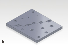
Download figure:
Standard image High-resolution image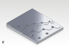
Fig. 10. Schemes of three growth modes: (a) hillocks; (b) hillocks and macrosteps; (c) macrosteps with flounces and step bunching effect; respective real images are presented in Fig. 5.
Download figure:
Standard image High-resolution imageThese three growth modes have never been observed for the crystallization in the Ga:Mg solution. In this case, a new material is grown by the macroscopically stable way only on the  surface of the HVPE-GaN seed. It suggests that the polarity of the GaN seed surface is determined and controlled by the Ga solution and its impurities. For applied temperature gradient, only macrosteps growth mode has been detected. The voids and/or gallium inclusions have never been found. Addition of Mg to the Ga solution may drastically change some properties of the solution, mainly its viscosity. Some changes in the solution's composition may prevent the formation of the voids and inclusions while maintaining the same growth rate. The disadvantage of the HNPS-MFS-GaN:Mg crystals is the precipitation of small magnesium oxide crystals. They are mainly formed at the interface between the FS HVPE-GaN seed and the new, pressure grown material. Some of them also exist in the volume of the HNPS-MFS-GaN:Mg crystal. The affinity of oxygen to magnesium seems to be so high that during crystallization process, especially at the beginning of the growth, the formation of MgO crystals takes place. Following that the crystals are overgrown by HNPS-MFS-GaN:Mg. Unfortunately, during the preparation of HNPS-MFS-GaN:Mg substrates the MgO crystals (or voids after them) can create some big pits in the nitride material.
The oxygen atoms in HNPS-MFS-GaN and in the HNPS-MFS-GaN:Mg crystals have to be originated from liquid gallium. An increase of the oxygen content in the GaN crystals with an increase of the growth temperature (see Fig. 6) results from a higher solubility of the oxygen in liquid gallium at high temperature and high pressure. For the highest temperatures the oxygen solubility limit in liquid gallium can be observed. Therefore, the oxygen concentration and its free carrier concentration in the HNPS-MFS-GaN crystals do not increase any further. The SIMS analysis showed that the magnesium concentration in the HNPS-MFS-GaN:Mg crystals is strictly the same as oxygen concentration [see Fig. 8(a)]. Thus, the magnesium impurity compensates oxygen donor in the pressure grown material. Therefore, these crystals are semi-insulating at room temperature, as well as at higher temperatures. It should be noted that for the same magnesium concentration in the solution and in the crystals, the resistivity depends on the growth temperatures. It is lower for crystals grown at low temperatures. It seems that it can be also associated with the oxygen concentration in the solution.
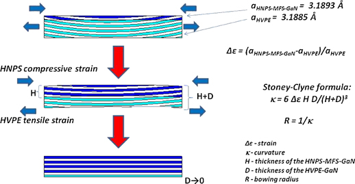
The formation of the n-type HNPS-GaN layer on the HVPE-GaN substrate (obtained from the MOCVD-GaN/sapphire template) can significantly change (improve) the bowing radius of the crystal. It is clearly possible if only the HVPE-GaN and the HNPS-MFS-GaN are elastically strained. Almost a total dissolution of the HVPE-GaN substrate helps to release the stress in HNPS-MFS-GaN. Therefore, the bowing radius of the HNPS-GaN crystal increases in comparison to the seed. As it is shown in Fig. 11, due to the difference in the a lattice constant between the HVPE-GaN and the HNPS-MFS-GaN, the pressure grown material is under compressive strain and the HVPE-GaN seed is under tensile strain during the crystallization process. The HVPE-GaN, however, dissolves from its  surface. On the other hand, the HNPS-MFS-GaN becomes thicker and thicker. Thus, the compressive strain for the HNPS-MFS-GaN has to be decreased in time and finally the pressure grown crystal, according to the Stoney-Clyne formula,48) can be structurally flatter.
Fig. 11. Model of the growing HNPS-MFS-GaN crystal's evolution in time; due to the difference in the a lattice constant of the HNPS-MFS-GaN and the HVPE-GaN seed the pressure grown material is under compressive strain and the HVPE-GaN seed is under tensile strain; if the HNPS-MFS-GaN and the HVPE-GaN are elastically strained the bowing radius of the final crystal increases according to the Stoney-Clyne formula48) presented in the figure.
Download figure:
Standard image High-resolution image
It should be mentioned that the X-ray rocking curve FWHM and the bowing radii of the HNPS-MFS-GaN:Mg crystals are not changed significantly, comparing to the HVPE-GaN seeds. However, the a lattice constant of the HNPS-MFS-GaN:Mg is the same as for the FS HVPE-GaN seed.36,49) Therefore, there is no difference in strains for these two layers. The FS HVPE-GaN seed is, then, structurally reproduced by the high pressure material.
4. Conclusions
State of the art of the high nitrogen pressure solution (HNPS) growth method has been described. Seeded growth by a multi-feed seed (MFS) configuration has been presented. The influence of structural quality of the seeds on structural quality of the new grown material has been demonstrated. It has been shown that the HNPS-MFS configuration involves the conversion of the free-standing HVPE-GaN crystals to the free-standing HNPS-MFS-GaN. These crystals are of a much higher quality than the seeds. The free standing HNPS-MFS-GaN crystals can be strongly n-type (GaN:O) or semi-insulating (GaN:Mg). They can also be prepared as substrates for the laser diodes (plasmonic substrates) or for the high electron mobility transistors (semi-insulating substrates), respectively. The only way to improve the structural quality of the HNPS-MFS-GaN is to use high quality HVPE-GaN crystals as seeds. The use of the FS HVPE-GaN crystals (obtained from ammono-GaN) as seeds for the HNPS growth method seems to be interesting and promising for producing high quality n-type and semi-insulating GaN crystals, and then substrates. On the other hand, it also seems that in order to improve the HNPS growth method a higher growth rate is necessary. It is believed that some changes in the properties of gallium solution should be carried out. The purpose of such changes is to increase the nitrogen solubility in liquid gallium, as well as convectional velocities in the solution. By adding sodium or lithium impurities to gallium one can obtain a solution (or a flux) of a lower density, modified viscosity and with an increase in the nitrogen solubility. An additional possibility can be a mechanical stirring of the solution, which has already been applied in the sodium flux GaN growth.50)
Acknowledgments
This research was supported by The National Centre for Research and Development: PBS 1/B5/7/2012 and by the European Union within the European Regional Development Fund, through grants: Innovative Economy (POIG.01.04.00-14-153/11) and Innovative Economy (POIG.01.01.02-00-008/08).
Biographies

Michal Bockowski received the M. Sc. Eng. in Solid State Physics from the Warsaw University of Technology (Poland), the Ph. D. in Chemistry of Solids 1995 from the University Montpellier II (France) and D. Sc. in Physics from the Institute of Physics Polish Academy of Sciences (Poland). He is currently the Research Associate of the Institute of High Pressure Physics of the Polish Academy of Sciences and the vice president of TopGaN Ltd. His main interests are related to nitride semiconductors. He is one of pioneers of high-pressure crystallization of nitride semiconductors.