
Abstract
In this paper, we give an overview of the recent progress in GaN-based high-electron-mobility transistors (HEMTs) developed for mainstream acceptance in the power electronics field. The comprehensive investigation of AlGaN/GaN HEMTs fabricated on a free-standing semi-insulating GaN substrate reveals that an extracted effective lateral breakdown field of approximately 1 MV/cm is likely limited by the premature device breakdown originating from the insufficient structural and electrical quality of GaN buffer layers and/or the GaN substrate itself. The effective lateral breakdown field is increased to 2 MV/cm by using a highly resistive GaN substrate achieved by heavy Fe doping. Various issues relevant to current collapse are also discussed in the latter half of this paper, where a more pronounced reduction in current collapse is achieved by combining two different schemes (i.e., a prepassivation oxygen plasma treatment and a field plate structure) for intensifying the mitigating effect against current collapse. Finally, a novel approach to suppress current collapse is presented by introducing a three-dimensional field plate (3DFP) in AlGaN/GaN HEMTs, and its possibility of realizing true collapse-free operation is described.
Export citation and abstract BibTeX RIS
1. Introduction
GaN-based high-electron-mobility transistors (HEMTs) have achieved continuous progress with the demonstration of promising low-loss and high-voltage switching capabilities for use in next-generation power electronics circuits. This is primarily due to their outstanding intrinsic material and device properties, such as a wide bandgap of 3.4 eV for stable high-temperature operation, a high breakdown electric field of more than 3 MV/cm for high-voltage operation, and a high electron mobility exceeding 1500 cm2 V−1 s−1 for low on-state resistance. In addition, a large conduction band offset between AlGaN and GaN along with polarization charges at the heterointerface induces high-density two-dimensional electron gas (2DEG) with a high mobility. By taking advantage of the high breakdown electric field of GaN, off-state breakdown voltages of over 1 kV have been achieved in GaN-based devices.1–17) Uemoto et al. reported a high breakdown voltage of 8.3 kV with an AlGaN/GaN HEMT having an AlN passivation fabricated on a sapphire substrate,4) and later updated their record value of maximum off-state breakdown voltage to 10.4 kV.5)
Despite those promising results on breakdown voltages, the measured lateral breakdown electric field in AlGaN/GaN HEMTs, defined as the measured off-state breakdown voltage divided by the gate-to-drain distance (Lgd), was typically around 1 MV/cm, which is significantly lower than the theoretically predicted value of 3.3 MV/cm. Such unexpectedly lower values in breakdown electric field have been reported with AlGaN/GaN HEMTs fabricated on different substrate materials, such as Si,9–11,13–15,17,18) sapphire,2–5) and SiC.1,8,12,16) So far, no clear explanation has been made regarding the discrepancy between the measured effective lateral breakdown field and the predicted value. This is partly because the quality of the buffer layer, which is inserted primarily to compensate the lattice mismatch between GaN and a foreign substrate material, was not sufficiently optimized for high-voltage operation. Srivastava et al. reported a substantial improvement using a novel local substrate removal technique, in which the Si substrate under the source-to-drain region was selectively removed by inductively coupled plasma (ICP) dry etching.9,10) The local removal of both Si substrate and related interfacial layers resulted in a high breakdown voltage of 2.2 kV, corresponding to a lateral breakdown field of 1.1 MV/cm. The results strongly suggest the importance of improving the quality of buffer and/or substrate materials to achieve even higher breakdown voltages as well as to improve the effective breakdown electric field in GaN-based electron devices.
Regarding the experimental evaluation of the breakdown electric field, more encouraging results have been reported in GaN p–n diodes19–24) and GaN vertical MOSFETs.25–28) Kizilyalli et al. extracted a critical electric field of more than 3.5 MV/cm from a vertical p–n diode fabricated on a free-standing GaN substrate.22) The use of a high-quality n-type GaN drift layer grown on a low-dislocation-density GaN substrate (104–106 cm−2) was found essential for achieving better breakdown characteristics. These results on GaN-based vertical power devices suggest that substantial improvements in the breakdown characteristics of lateral HEMTs would be possible by fabricating devices on a semi-insulating free-standing GaN substrate.
In addition to the improvement in breakdown characteristics, the reduction in the on-state resistance Ron is also of special importance for next-generation power applications. Although the access and channel resistances of AlGaN/GaN HEMTs are known to be minimized by the benefit of the high electron mobility of 2DEG, this advantage is guaranteed only under static bias conditions. During drain current transients from off-state (pinch-off region) to on-state (linear region), the on-state resistance is often heavily degraded as compared with its static value. This phenomenon of increased dynamic Ron and the subsequent decreased on-state drain current is referred to as "current collapse" and considered as one of the most serious problems to be solved for practical power switching applications of GaN-based HEMTs.
Historically speaking, similar behaviors of dynamic drain current reduction after high-voltage application were observed in n-channel silicon MOSFETs29) and CdSe thin-film transistors (TFTs).30) Heavily distorted drain current–voltage (I–V) characteristics were also observed in AlGaAs/GaAs HEMTs when they were cooled to cryogenic temperatures.31–33) This distortion was found to be a temporary phenomenon and could be recovered by shining light onto the devices, suggesting that the drain current "collapse" was due to the injection of hot electrons and eventual trapping in the AlGaAs layer.33,34) Similarly, trapping phenomena, called gate lag35,36) and drain lag,37,38) became well known to occur at room temperature in GaAs MESFETs and AlGaAs/GaAs HEMTs, leading to premature power saturation in high-frequency power operation. Asano et al. reported the first application of a field plate to avoid undesirable trapping effects in power GaAs MESFETs and AlGaAs/GaAs HEMTs.39,40)
With the earlier knowledge of trap-related issues in GaAs-based devices, similar problems occur in GaN-based devices, and to make situations more complicated, GaN has a wider bandgap, which admits a variety of deeper traps with longer associated time constants for carrier emission. Furthermore, the high critical electric field of GaN facilitates device operation up to hundreds of volts, leading to the extreme charge injection and trapping of carriers. These intrinsic properties of GaN may make the trap-related collapse issue more noticeable.
The earliest report of current collapse in AlGaN/GaN-based devices was by Khan et al.,41) and attributed the current collapse to the trapping of hot electrons in the AlGaN layer. Subsequent studies identified that trapping in the GaN channel42) and hot electron injection into GaN buffer layers43,44) were also responsible for the observed current dispersion. Meanwhile, the drain current compression observed for GaN-based HEMTs operated at microwave frequencies was highly dependent on gate voltage, which suggested that carrier trapping likely occurred either in the AlGaN barrier or AlGaN surface.45)
To explain the current collapse observed in AlGaN/GaN HEMTs subjected to high drain biases with a pinch-off gate bias, Vetury et al. introduced the "virtual gate" model related to surface trapping on the drain side of the gate edge.46) This surface trap model is widely supported by a number of experimental observations, in which current collapse is mitigated by proper surface passivation with SiN,47) SiO2,48) Al2O3,49) MgO,50) and AlN.51) The charge dynamics of surface states due to the trapping/detrapping of carriers are assumed to directly affect the channel 2DEG density, resulting in the change in the on-state resistance and/or drain current. Additionally, several groups52–58) have adopted the field-plate technique to relax the electric field in the gate-to-drain region. The weakened driving force for charge injection into trap centers eventually resulted in the mitigation in current collapse. However, no single approach has ever succeeded in the complete suppression of current collapse in power GaN-based HEMTs operated at sufficiently high frequencies and bias voltages.
The first half of this paper is devoted to describing the comprehensive characterization of breakdown voltages measured on a series of AlGaN/GaN HEMTs fabricated on a free-standing semi-insulating GaN substrate. The measured breakdown voltages and the extracted lateral breakdown field are characterized in terms of intrinsic and extrinsic structural parameters of the fabricated devices. The possible mechanisms responsible for parasitic leakages and premature device breakdown will be discussed. The latter half of this paper is intended to describe several approaches developed for suppressing current collapse, including high-pressure water vapor annealing (HPWVA), oxygen plasma treatment, GaN cap, field plate (FP), and multimesa channel (MMC). Furthermore, advanced approaches aiming for a more pronounced reduction in current collapse are also presented by combining the two schemes mentioned above to enhance the mitigating effect against current collapse. Finally, a novel approach to reduce current collapse is presented by introducing a three-dimensional field plate (3DFP) in AlGaN/GaN HEMTs, and its possibility of realizing true collapse-free operation is discussed.
2. Breakdown voltages in AlGaN/GaN HEMTs
2.1. Device structure and fabrication
The AlGaN/GaN heterostructures were grown by metal–organic chemical vapor deposition (MOCVD) on 2-in. free-standing GaN substrates. The GaN substrate, prepared by hydride vapor phase epitaxy (HVPE), was doped with Fe with a doping concentration of about 1 × 1018 cm−3 to ensure a semi-insulating property. The threading dislocation density of the starting GaN substrate was nominally 106 cm−2. The epitaxial structure consists of a 25-nm-thick AlGaN barrier layer, a 900-nm-thick undoped GaN channel layer, and a 300-nm-thick Fe-doped GaN buffer layer. The Al content in the AlGaN barrier layer was 0.2.
Figure 1 shows the simplified schematic of the fabrication process and subsequent device structure. The device fabrication started with mesa isolation using BCl3/Cl2-based ICP reactive ion etching (RIE). To study the effect of mesa isolation on breakdown characteristics, the mesa etching depth was varied from 200 to 1400 nm. Then, source and drain ohmic contacts were formed by evaporating Ti/Al/Mo/Au metal stacks, followed by rapid thermal annealing at 850 °C for 30 s in an N2 atmosphere. Ni/Au was then deposited as Schottky gate electrodes. Finally, the devices were passivated with a 150 nm sputter-deposited SiN film. The gate length (Lg), gate width (Wg), and gate-to-source distance (Lgs) were fixed at 3, 100, and 3 µm, respectively, while the gate-to-drain distance (Lgd) was varied from 5 to 200 µm. Figure 2 shows schematic diagrams of AlGaN/GaN HEMTs fabricated on a semi-insulating GaN substrate with mesa depths of 200, 1000, and 1400 nm, where the mesa surfaces are located on the undoped GaN channel, on the Fe-doped GaN buffer layer, and on the semi-insulating GaN substrate, respectively.
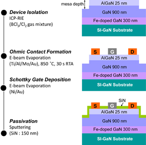
Fig. 1. Schematic of fabrication process and subsequent device structure of investigated AlGaN/GaN HEMTs.
Download figure:
Standard image High-resolution image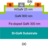
Download figure:
Standard image High-resolution image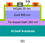
Download figure:
Standard image High-resolution image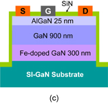
Fig. 2. Schematic cross-sectional view of AlGaN/GaN HEMTs fabricated on semi-insulating GaN substrate with different mesa depths of (a) 200, (b) 1000, and (b) 1400 nm, where the mesa surfaces fall on undoped GaN channel, Fe-doped GaN buffer layer, and semi-insulating GaN substrate, respectively.
Download figure:
Standard image High-resolution image2.2. Dependence of breakdown voltage on gate-to-drain distance
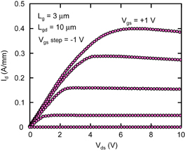
Figure 3 shows the output and transfer current–voltage characteristics (Id–Vds and Id–Vgs) of the AlGaN/GaN HEMT fabricated on a semi-insulating GaN substrate with a mesa depth of 200 nm and Lgd = 10 µm. The device exhibited a maximum drain current of 0.4 A/mm, a threshold voltage of −2.9 V, an on-state resistance of 10 Ω-mm, an on/off current ratio of 109, and a subthreshold swing of 73 mV/dec. Overall DC characteristics were almost the same as those for the HEMT fabricated on a SiC substrate with essentially the same epitaxial structures and device geometry.
Download figure:
Standard image High-resolution image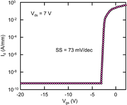
Fig. 3. Output and transfer I–V characteristics of AlGaN/GaN HEMT fabricated on semi-insulating GaN substrate with mesa depth of 200 nm and gate-to-drain distance (Lgd) of 10 µm.
Download figure:
Standard image High-resolution imageFigure 4 shows the off-state breakdown voltage as a function of Lgd for AlGaN/GaN HEMTs with a mesa depth of 200 nm. The off-state breakdown voltage, defined at a drain current of 1 mA/mm, exhibited a linear increase with the increase in Lgd and reached 3.8 kV at Lgd = 60 µm, beyond which the device showed saturation in the breakdown voltage at approximately 4 kV. From the gradient in the linear region of this plot, the effective breakdown electric field was derived to be 0.6 MV/cm, which is slightly lower than those reported in AlGaN/GaN HEMTs fabricated on foreign substrates such as Si,9–11,13–15,17,18) sapphire,2–5) and SiC.1,8,12,16) Careful observations revealed that catastrophic breakdown was dominant in the linear region up to Lgd = 60 µm, while the breakdown voltage was determined by the increased leakage current in the saturation region beyond Lgd = 60 µm. These results suggest the presence of parasitic leakage paths for devices with a mesa depth of 200 nm.
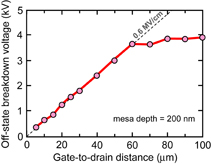
Fig. 4. Off-state breakdown voltage as function of Lgd for AlGaN/GaN HEMTs with mesa depth of 200 nm.
Download figure:
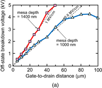
Standard image High-resolution imageA question therefore arises whether the additional leakage paths originate from the intrinsic (in the mesa isolation region) or extrinsic (outside the mesa isolation region) part of the HEMT device. To address this issue, devices with deeper mesa isolation etching were subjected to similar breakdown voltage measurements in terms of Lgd. Figure 5(a) shows the off-state breakdown voltage as a function of Lgd for AlGaN/GaN HEMTs with mesa depths of 1000 and 1400 nm. For devices with a mesa depth of 1000 nm, where the surface of mesa isolation is located on the Fe-doped GaN buffer layer, the off-state breakdown voltage was linearly increased up to Lgd = 60 µm and then became saturated at approximately 4 kV. The total breakdown behavior for the mesa depth of 1000 nm was essentially the same as that for the mesa depth of 200 nm, indicating that the presence of a 900 nm GaN channel layer in the mesa area does not induce additional leakage current components. Meanwhile, an entirely different breakdown behavior was observed for the device with a mesa depth of 1400 nm, where the surface of the mesa isolation is located on the semi-insulating GaN substrate. The 1400 nm mesa-etched devices demonstrated an almost linear increase in the breakdown voltage up to a measurement setup limit of 5 kV. From the slope of the dependence, an effective lateral breakdown field of 1 MV/cm was extracted. This increase in the breakdown field is primarily due to the removal of the Fe-doped GaN buffer layer, suggesting that the presence of the GaN buffer layer permits some premature breakdown and/or flow of non-negligible leakage current in the extrinsic part of the device, as illustrated in Fig. 5(b).
Download figure:
Standard image High-resolution image
Fig. 5. (a) Off-state breakdown voltage as a function of Lgd for AlGaN/GaN HEMTs with different mesa depths of 1000 and 1400 nm. (b) Schematic drawing of possible leakage current components under off-state conditions. One is intrinsic leakage current inside mesa region and the other is extrinsic leakage current outside mesa region.
Download figure:
Standard image High-resolution image2.3. Effect of mesa depth
To understand the effect of mesa etching depth in more detail, two-terminal I–V characteristics were measured between ohmic contact electrodes formed on the same AlGaN/GaN heterostructures. Each ohmic electrode, having a square shape with a width of 100 µm, was mesa isolated by varying the mesa depth from 200 to 5000 nm. Breakdown characteristics were measured between ohmic electrodes separated with distances of 20 and 35 µm as a function of mesa etching depth. As shown in Fig. 6, a steplike increase in breakdown voltage is clearly observed in the mesa depth region between 1000 and 1400 nm. The breakdown voltage became almost constant at mesa depths larger than 1400 nm, where the GaN buffer layer was completely etched away. These results confirm that a higher resistivity in the GaN buffer layer is of substantial importance to achieve better breakdown characteristics in an AlGaN/GaN HEMT structure on a free-standing GaN substrate.
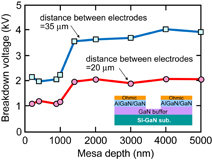
Fig. 6. Breakdown voltage as a function of mesa depth for two pairs of ohmic electrodes: one pair separated by 20 µm and the other by 35 µm.
Download figure:
Standard image High-resolution image2.4. Effect of Fe doping in GaN substrate
From a series of breakdown measurements for AlGaN/GaN HEMTs fabricated on a semi-insulating GaN substrate with different mesa etching depths, it was found that the highest available breakdown voltage seemed to be restricted by the breakdown and/or the leakage current in a semi-insulating GaN substrate under high applied electric field conditions. To confirm this limitation, the breakdown characteristics were measured between ohmic contact electrodes, which were directly formed on a GaN substrate. Measurements were made on a HVPE-grown free-standing GaN substrate with an Fe doping concentration of 1 × 10¹⁸ or 9 × 1019 cm−3. Results are shown in Fig. 7, where measured breakdown voltages are plotted as a function of ohmic-to-ohmic distance varied from 4 to 25 µm. For both semi-insulating GaN substrates, the breakdown voltage increased linearly with the increase in the ohmic-to-ohmic distance. Note that an effective lateral breakdown field of as high as 2 MV/cm was achieved for the heavily Fe-doped GaN substrate (9 × 1019 cm−3). This value is, to the best of the authors' knowledge, the highest effective breakdown field ever recorded on the horizontal GaN devices. These results strongly suggest that a higher lateral breakdown field may be achievable by further increasing the resistivity of a semi-insulating GaN substrate through the reduction of the background donor concentration and/or the defect density in a GaN substrate.

Fig. 7. Breakdown voltage as a function of ohmic-to-ohmic distance of ohmic electrodes formed on top of two types of GaN substrate with different degrees of unintentional carrier compensation: one has an Fe doping concentration of 1 × 1018 cm−3 while the other is heavily compensated with 9 × 1019 cm−3 Fe doping concentration.
Download figure:
Standard image High-resolution imageOne might think that SiC or sapphire would be more preferable as a starting substrate to achieve higher values in the effective lateral breakdown field in AlGaN/GaN HEMTs because the material has more perfect semi-insulating properties. However, this is not true because more complicated and thicker buffer layers are usually necessary to grow high-quality GaN-based heterostructures. Only a free-standing GaN substrate can permit the growth of very thin buffer GaN layers with controlled high-resistivity properties, which are of particular importance to suppress parasitic leakage current and/or premature breakdown.
3. Suppression of current collapse in AlGaN/GaN HEMTs
3.1. Device fabrication
Current collapse is another major hurdle that needs to be properly addressed before the wide-scale adoption of AlGaN/GaN HEMTs for power electronics. This section is devoted to summarizing our recent efforts in exploring alternative solutions towards the suppression of current collapse, such as high-pressure water vapor annealing (HPWVA), oxygen (O2) plasma treatment, introduction of FP, and using 3DFP structures. For gauging the effectiveness of these different approaches to current collapse, the performance of each prototype device employing the above-mentioned schemes was compared with that of a reference device fabricated on the same substrate. This is to avoid process-specific variations in contact resistances and other relevant device parameters that may mask the effect of the different approaches on device performance being measured. Reference devices were fabricated using the same process shown in Fig. 1. For each prototype device employing one of the above-mentioned schemes, additional steps were inserted into the fabrication process, as will be discussed later accordingly. For the purpose of current collapse evaluation, devices were fabricated using an Al0.2Ga0.8N/GaN heterostructure grown on a 4H-SiC substrate by MOCVD. The epitaxial structure consists of a 25-nm-thick AlGaN barrier layer, a 500-nm-thick undoped GaN channel layer, and an AlN nucleation layer (NL). The AlN NL facilitates high-quality GaN heteroepitaxy by accommodating the lattice mismatch between the GaN layer and the underlying SiC substrate. Unless otherwise specified, for all devices, Lgs, Lg, Lgd, and Wg were 3, 3, 10, and 100 µm, respectively.
3.2. Measurement and characterization of current collapse
Figure 8 outlines the important details of the current collapse evaluation method performed on the devices. As given in Fig. 8(a), a drain bias voltage (VDD) provided by a power supply (Texio PA600-0.1B) was used in series with a load resistance (RL), while a train of gate pulses from a pulse generator (Iwatsu DG 8000) was applied to the gate. The values of VDD and RL were appropriately chosen so that the resulting load line intersects the Id–Vds curve at a point below 1/4 of the maximum drain current. This ensured that Ron being measured was within the linear region. During the off-state, VDD supplies the off-state drain voltage stress Vds_off. For mimicking a typical operation under which devices in power switching circuits are subjected, values of the gate voltage (Vgs) alternating between −5 V (off-state) and +1 V (on-state) were applied to the gate terminal as shown in Fig. 8(b).
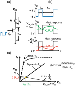
Fig. 8. Schematic of (a) circuit used for current collapse evaluation showing the drain bias voltage (VDD), which provides electrical stress (Vds_off) during device off-state, (b) drain current and voltage waveforms, and (c) graphical definition of load lines and dynamic Ron.
Download figure:
Standard image High-resolution imageFor brevity, we first define ton as a preselected fixed time interval following the rising edge of the gate pulse, during which the device is in the "on" state as illustrated in Fig. 8(b). In other words, ton is the elapsed time after switching the device from off- to on-state. After every ton, the corresponding Vds(ton) and Id(ton) were recorded using an oscilloscope (LeCroy WaveRunner 204Xi-A) and used to compute the dynamic Ron as illustrated in Fig. 8(c). For representing current collapse quantitatively, we used the normalized dynamic Ron (NDR), which is defined as the ratio of dynamic Ron to static Ron. A higher NDR indicates a higher degree of current collapse. Using the electrical circuit given in Fig. 8(a), we can then monitor how the NDR of the devices evolves with the variation in either Vds_off (method 1) or ton (method 2) for current collapse evaluation. The dependence of NDR on ton can also be used to estimate the energy levels of the traps responsible for the current collapse as discussed below.
The general expression for Ron is given by the following relationship:

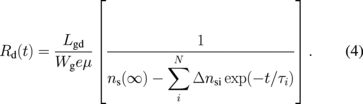
where Rc, Rs, Rch, and Rd represent contact resistance, source access resistance, channel resistance, and drain access resistance, respectively. According to the model by Vetury et al.,46) current collapse is due to the trapping of injected electrons on the drain side of the gate edge during the off-state, which eventually depletes the underlying 2DEG in this portion of the gate-to-drain access region, consequently increasing the dynamic Ron, i.e., current collapse. After switching the device from off- to on-state, the drain access resistance transient Rd(t) can be mathematically given by

where
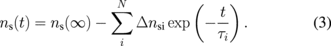
Here, t is the elapsed time after switching the device from off- to on-state. ns(t) and ns(∞) represent the effective drain access region 2DEG density at time t and t = ∞ (static), respectively. As given by Eq. (3), the difference in ns(∞) and ns(t) can be given by the sum of pure exponential terms, where Δnsi represents the effective sheet density of trapped electrons in the ith trap with a corresponding emission time constant τi immediately prior to switching the device to the on-state. As t increases, the sum of the exponential terms representing the effective density of trapped electrons approaches zero. Substituting Eq. (3) into Eq. (2) yields
Applying Taylor series approximation on the expression inside the parenthesis, one can easily obtain
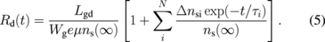
Using Eq. (5), we can rewrite Eq. (1) into
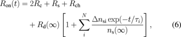
where

From the definition of NDR, we can finally obtain

where αi is the fractional contribution of the ith component and is given by
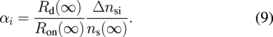
Note that αi is directly proportional to Δnsi, which is the effective sheet density of trapped electrons in the ith trap immediately prior to switching the device from off- to on-state, and is related to the ith trap density itself. In addition, it is worth mentioning that Eq. (8) is very similar in form to the transient drain current expression proposed by Joh and del Alamo.59)
The experimentally measured ton dependence of NDR can be fitted with Eq. (8) to extract the τi of the ith trap level, from which the corresponding (EC − Et) energy value can be obtained using the Shockley–Read–Hall (SRH) statistics relationship
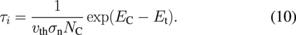
Here, vth is the electron thermal velocity, σn is the capture cross section, and NC is the effective density of states at the conduction band edge.
3.3. Effect of high-pressure water vapor annealing
There is somewhat a general agreement in the literature that current collapse is predominantly, if not solely, due to trapping on the AlGaN surface. Needless to say, one of the earliest proven approaches against current collapse is AlGaN surface passivation.47) Because of the high sensitivity of current collapse to AlGaN surface condition, different prepassivation treatment methods should also be explored as alternative solutions. Sameshima and co-workers were the first to demonstrate the applicability of high-pressure water vapor annealing (HPWVA) to semiconductor process technologies.60,61) They reported improved properties of SiO2 films and SiO2/Si interfaces subjected to HPWVA. It was also found by Punchaipetch et al.62) that HPWVA was able to raise the quality of hafnium silicate (HfSixOy), which is one of the high-κ gate dielectric materials used in modern semiconductor devices. Recently, Yoshitsugu et al.63) have demonstrated the effectiveness of HPWVA in improving the quality of Al2O3 gate dielectric in n-GaN MOS capacitors. Following these pioneering works, a significant reduction in current collapse was also achieved in AlGaN/GaN HEMTs using HPWVA.64) The HPWVA process was carried out prior to the SiN passivation step. Devices to be subjected to HPWVA were initially set in a sealed chamber. Together with the devices, a predetermined volume of pure water was placed inside the chamber. This volume of water corresponded to the desired pressure at a given setting temperature. A water vapor pressure of 0.5 MPa was used in this work. The chamber was then sealed and heated to a desired annealing temperature for a particular length of time, and then allowed to cool naturally. With a fixed annealing time of 30 min, three different HPWVA conditions corresponding to annealing temperatures of 200, 300, and 400 °C were used.
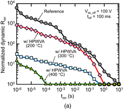
Figure 9(a) shows the measured NDR as a function of ton of the reference and HPWVA-processed devices. As expected, NDR decreased with increasing ton for all devices. This is because a longer ton allowed more time for the emission of trapped electrons, resulting in a greater recovery of dynamic Ron. More importantly, NDR decreased with increasing annealing temperature for all HPWVA-processed devices as compared with the reference device, suggesting the efficacy of HPWVA in alleviating current collapse.
Download figure:
Standard image High-resolution image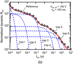
Fig. 9. NDR as a function of on-time (ton) of (a) reference and HPWVA-processed AlGaN/GaN HEMTs at fixed drain bias voltage (Vds_off) of 100 V and off-time (toff) of 100 ms, and (b) reference device with extracted six exponential terms for deep-level traps plotted by dashed curves.
Download figure:
Standard image High-resolution imageBy fitting the measured NDR–ton curve with Eq. (8) by the least-squares method, six deep level traps were detected from the reference device, as illustrated in Fig. 9(b). In this figure, extracted exponential terms are plotted by dashed curves, each of which represents a particular trap level. On the other hand, only two levels were detected from the 400 °C HPWVA-processed device. Table I summarizes the extracted values of τi and αi of these trap levels. Assuming vth of 2.6 × 107 cm/s, σn of 1.0 × 10⁻¹⁵ cm2, and NC of 2.2 × 1018 cm−3, the trap energy level (EC − Et) values given in the fourth column of Table I were obtained using Eq. (10).
Table I. Extracted trap energy levels (EC − Et) from reference (w/o HPWVA) and HPWVA-processed (400 °C) devices.
| Device | αi | τi (s) | EC − Et (eV) |
|---|---|---|---|
| Reference (w/o HPWVA) | 1.2 × 10⁴ | 8.0 × 10⁻⁷ | 0.28 |
| 1.1 × 10³ | 2.4 × 10⁻⁵ | 0.37 | |
| 1.0 × 10³ | 7.1 × 10⁻⁴ | 0.45 | |
| 88 | 2.5 × 10⁻² | 0.54 | |
| 38 | 1.8 × 10⁻¹ | 0.59 | |
| 12 | 9.0 × 10⁻¹ | 0.64 | |
| HPWV-annealed (400 °C) | 25.9 | 7.4 × 10⁻⁷ | 0.28 |
| 7.5 | 2.5 × 10⁻⁵ | 0.37 |
The (EC − Et) values ranged from 0.28 to 0.64 eV and from 0.28 to 0.37 eV for the reference and the HPWVA-processed device, respectively. The corresponding αi of traps after HPWVA were orders of magnitude lower than those of the reference device. Subsequent X-ray photoelectron spectroscopy (XPS) analyses revealed the chemical blue shift of Ga Auger LMM signals from the HPWVA-processed AlGaN surface relative to those of the reference sample, suggesting the formation of the surface oxide layer of Ga2O3 and possibly interfacial Ga2O sub-oxide, which was reported to be essential for achieving low defect density in III–V surfaces.65–68) On a final note, HPWVA is considered to promote oxygen incorporation, which leads to the formation of surface oxide suitable for device passivation, occupation of near-surface nitrogen vacancies, and termination of unbounded near-surface Ga and Al atoms.16) All of these effectively decreased the number of surface states that trap carriers, leading to a highly reduced current collapse.
3.4. Effect of O2 plasma treatment and GaN cap
Various gas-plasma treatments of AlGaN surface were reported to be effective in mitigating current collapse.69–71) Recently, a significant reduction in current collapse has been demonstrated for O2 plasma-treated AlGaN/GaN HEMTs as evidenced by highly reduced NDR in these devices over that of a reference device.72) The AlGaN surface of the devices was exposed to O2 plasma with an RF power of 100 W and an exposure time of 60 s. This was carried out prior to a SiN passivation step of the fabrication process shown in Fig. 1. Meanwhile, there were also reports that an epitaxial GaN cap layer was capable of reducing current collapse.73–77) Aware of these reports, we also applied O2 plasma surface treatment to the fabrication of AlGaN/GaN HEMTs having a GaN cap layer. Four different devices with the following features were fabricated: (1) without GaN cap and without O2 plasma treatment as reference device; (2) without GaN cap and with O2 plasma treatment; (3) with GaN cap and without O2 plasma treatment; and (4) with GaN cap and with O2 plasma treatment. Figure 10 presents the NDR values of the four devices as a function of ton. Careful investigation of the resulting NDR–ton curves led to the following two important conclusions: (1) O2 plasma treatment was more effective than the GaN cap in suppressing current collapse and (2) the GaN cap layer approach was redundant and insignificant to current collapse mitigation when used in combination with O2 plasma treatment. These key findings suggest that by using only O2 plasma treatment, one can avoid the problems associated with surface GaN layers, such as increased leakage current and difficulty in obtaining good ohmic contacts.76,77) Following the fitting procedure of NDR–ton curves and analysis using SRH statistics, the characteristic τi's and the equivalent energy levels of traps present in each device were extracted. The results, summarized in Table II, suggest that the O2 plasma treatment is more effective than the GaN cap approach because the O2 plasma treatment leads to a significant reduction in surface trap densities, as suggested by its smaller αi values. Moreover, it also completely eliminated two of the deepest trap levels located at ∼0.62 and ∼0.67 eV. The GaN cap approach, on the other hand, only eliminated the deepest trap level at ∼0.67 eV. The more pronounced current collapse suppression in O2-plasma-treated devices, with or without GaN cap, was likely due to the formation of surface oxide, the termination of the near-surface Ga and Al atoms, and the occupation of nitrogen vacancies.16) These suppositions were supported by data from XPS investigations, which indicated oxygen atom incorporation and the subsequent formation of a 2-nm-thick surface oxide after O2 plasma exposure.

Fig. 10. NDR as a function of on-time (ton) of HEMT 1 (reference), HEMT 2 (with O2 plasma treatment, without GaN cap), HEMT 3 (without O2 plasma treatment, with GaN cap), and HEMT 4 (with O2 plasma treatment, with GaN cap) at fixed drain bias voltage (VDD = Vds_off) of 100 V and off-time (toff) of 100 ms.
Download figure:
Standard image High-resolution imageTable II. Device description and respective extracted trap energy levels (EC − Et).
| Device | O2 plasma treatment | GaN cap | αi | τi (s) | EC − Et (eV) |
|---|---|---|---|---|---|
| HEMT 1 (reference) | NO | NO | 4968 | 5.66 × 10⁻⁷ | 0.27 |
| 269 | 1.80 × 10⁻⁵ | 0.36 | |||
| 294 | 2.68 × 10⁻³ | 0.49 | |||
| 142 | 3.95 × 10⁻² | 0.56 | |||
| 24 | 3.97 × 10⁻¹ | 0.62 | |||
| 3.6 | 2.72 × 100 | 0.67 | |||
| HEMT 2 | YES | NO | 20 | 8.31 × 10⁻⁷ | 0.28 |
| 6.2 | 3.89 × 10⁻⁵ | 0.38 | |||
| 4.3 | 2.21 × 10⁻³ | 0.48 | |||
| 3.0 | 1.03 × 10⁻¹ | 0.58 | |||
| HEMT 3 | NO | YES | 178 | 8.31 × 10⁻⁷ | 0.28 |
| 32 | 3.89 × 10⁻⁵ | 0.38 | |||
| 27 | 5.77 × 10⁻³ | 0.51 | |||
| 30 | 8.53 × 10⁻² | 0.58 | |||
| 12 | 5.83 × 10⁻¹ | 0.63 | |||
| HEMT 4 | YES | YES | 20 | 1.22 × 10⁻⁶ | 0.29 |
| 6.0 | 2.18 × 10⁻⁵ | 0.36 | |||
| 4.0 | 3.93 × 10⁻³ | 0.50 | |||
| 2.3 | 8.53 × 10⁻² | 0.58 |
3.5. Effect of field plate
The use of the FP structure in AlGaN/GaN HEMTs dates back from the early 2000s. Ando et al. were the first to demonstrate high-voltage and high-efficiency microwave power performance using gate-FP in AlGaN/GaN HEMTs.52) They already noticed experimentally the importance of gate-FP in reducing current collapse as well as in improving device breakdown characteristics. Using the same FP technology, Okamoto et al. achieved the first over 200 W one-chip microwave power operation at 2 GHz.53) Since then, a number of papers have been published reporting that FP in AlGaN/GaN HEMTs is effective in enhancing device breakdown voltages.54–57) The FP structure redistributes the electric field profile along the drain access region, leading to a reduced electric field peak near the drain side of the gate edge and eventual breakdown voltage enhancement. Therefore, in principle, current collapse, which is considered to be due to trapping on the AlGaN surface of injected electrons from the metal gate, should also be reduced by the introduction of FP. Saito et al. reported improved collapse behaviors of the dual-FP HEMT over the single-FP device and attributed this difference to the leveled electric field distribution in the gate-to-drain region under off-state high-voltage biasing conditions.55)
The beneficial FP effects on current collapse were experimentally verified not only during the off-state but also during the on-state in the power switching operation. Hasan et al. fabricated an AlGaN/GaN HEMT with a gate-FP, as illustrated in Fig. 11, and measured the dynamic Ron as a function of on-state Vgs from −1 to +1 V.58) As clearly shown in Fig. 12, applying a more positive on-state Vgs resulted in the greater reduction of current collapse for the gate-FP device, but no such gate-bias dependence was observed for the standard HEMT without FP. Note that with decreasing on-state Vgs to −1 V, the NDR of the gate-FP HEMT approaches that for the HEMT without FP. This result revealed that the gate-FP has an important effect on current collapse during the on-state. Through the field-effect charge control of the gate-FP on channel electrons, the positively biased gate-FP is particularly effective in instantly recovering the partial depletion of channel electrons, which was caused by electron trapping during the off-state. Such beneficial effect during the on-state is peculiar to the gate-FP and would not be expected for the source-FP.
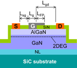
Fig. 11. Schematic cross-sectional view of field-plated AlGaN/GaN HEMT illustrating field plate length (LFP) and its relationship with relevant device parameters.
Download figure:
Standard image High-resolution image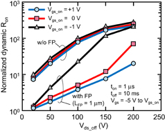
Fig. 12. NDR as a function of off-state drain bias voltage (Vds_off) of reference (without FP) and field-plated devices with varying on-state gate voltage (Vgs_on).
Download figure:
Standard image High-resolution image3.6. Combination of O2 plasma treatment and field plate
Aiming for a true "collapse-free" operation, attempts of combining different approaches against current collapse were also reported. It was suggested that using simultaneously two different approaches in mitigating current collapse did not necessarily guarantee a cumulative effect.72) To put it explicitly, it was found that the GaN cap layer contributed no further reduction in current collapse in the devices already subjected to O2 plasma treatment. Another report described a systematic investigation of the combined effect of O2 plasma treatment and FP structure on current collapse.78) For that purpose, four different devices with the following features were fabricated: (1) reference, (2) with FP, (3) with O2 plasma treatment, and (4) with FP and with O2 plasma treatment, referred as HEMT A, B, C, and D, respectively. For the O2-plasma-treated devices, the AlGaN surface was subjected to O2 plasma treatment using the same plasma power of 100 W and exposure time of 60 s before SiN passivation. Figure 13 shows NDR as a function of Vds_off. As expected, all devices exhibited the increasing trend of current collapse with increasing Vds_off. It was found that the O2 plasma treatment approach led to a stronger degree of current collapse suppression over the FP approach. Interestingly, the device with both FP and O2 plasma treatment showed the lowest degree of current collapse, indicating the cumulative effect of FP and O2 plasma treatment approaches in weakening current collapse. Asubar et al. explained that the effectiveness of the combined schemes was due to the fact that each scheme dealt with current collapse in a different way.78) While O2 plasma treatment reduced or eliminated surface trap densities responsible for current collapse, the FP structure modified the driving forces directly affecting the trapping and detrapping processes connected with current collapse.53–56)
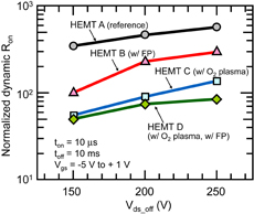
Fig. 13. NDR as a function of off-state drain bias voltage (Vds_off) of HEMT A (reference), HEMT B (without O2 plasma treatment, with FP), HEMT C (with O2 plasma treatment, without FP), and HEMT D (with O2 plasma treatment, with FP).
Download figure:
Standard image High-resolution image3.7. Multimesa channel
The multimesa-channel (MMC) AlGaN/GaN HEMT, schematically illustrated in Fig. 14, was an interesting structure-based approach of mitigating current collapse. The MMC device was fabricated by etching periodic trenches to form multiple mesas under the metal gate,79,80) hence the name multimesa channel. Each mesa channel, formed by electron beam lithography, was designed to have a width (Wtop) of less than 100 nm. The resulting structure facilitated the modulation of 2DEG not only through the top but also through the sidewalls, improving the device gate control over the drain current.81) Ohi et al. found that the device was less sensitive to changes in drain access resistance brought about by increasing LGD or trapping, and therefore less susceptible to current collapse.82,83) They argued that this was due to the much higher resistance of the mesa channel compared with that of the drain access region. This device, however, had a drawback of decreased net drain current per chip size due to the etching of active sections of the channel to form the trenches.
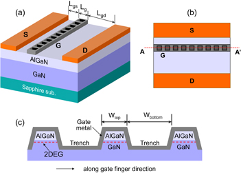
Fig. 14. Schematic illustration of MMC AlGaN/GaN HEMTs: (a) bird's eye view, (b) plan view, and (c) cross-sectional diagram along the cut-plane A–A' shown in (b).
Download figure:
Standard image High-resolution image3.8. Three-dimensional field plate structure
As discussed in the previous section, field-plate technology is well recognized as a powerful tool to achieve reduced current collapse without inducing any adverse effects in the device DC characteristics. However, a true collapse-free operation has not yet been established. Since the gate-FP in AlGaN/GaN HEMTs is proven effective to achieve significant current collapse reduction, enhancing the charge-control ability of the gate-FP would help maximize the efficiency of current collapse suppression. Meanwhile, it was verified that the addition of the lateral field effect in the configuration of the multimesa channel was effective in reducing current collapse. However, the removed section in the channel region reduced the effective active device width, leading to the decrease in the total drain current. This means eventual degradation in the on-resistance per chip size, which is of course detrimental for power device applications.
A new type of field plate device was developed with a view of intensifying the current collapse mitigating effect by FP. The structure is schematically illustrated in Fig. 15, in which multiple grooves were selectively fabricated in the field-plate area outside the channel region to avoid the sacrifice in total drain current normally inherent in MMC and trigate devices.84) The developed HEMT with 3DFP, also referred to as a multi-grooved field plate (MGFP), exhibited almost collapse-free operation with essentially negligible penalty in the total drain current density. Typical values of groove length, width, depth, and spacing were 2.5, 0.3, 0.2, and 0.9 µm, respectively. Figure 16 compares NDR as a function of Vds_off of the reference device (without FP) and the 3DFP HEMT at different values of on-state gate voltage (Vgs_on). The reference device exhibited almost overlapping NDR–Vds_off curves with varying Vgs_on, whereas the 3DFP HEMT showed NDR–Vds_off curves highly sensitive to the applied Vgs_on. For the 3DFP HEMT, at a given Vds_off, a more positive Vgs_on resulted in a lower NDR, a trend typically observed from gate-FP devices as discussed above. However, this tendency of decreasing NDR, and therefore weakening current collapse with increasing Vgs_on, was clearly more pronounced in the 3DFP HEMT. The resulting side-wall structures confined in the FP area, which allows not only vertical, but also lateral "field-effect action" during the on-state, helped in the faster recovery of trapped electrons responsible for current collapse, thereby intensifying the FP mitigating effect. As shown in Fig. 16, the 3DFP-HEMT exhibited an NDR value of essentially equal to 1 even at Vds_off of as high as 150 V, suggesting that this device may hold the key toward true "collapse-free" operation.
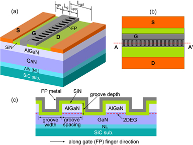
Fig. 15. Schematic illustration of 3DFP AlGaN/GaN HEMTs: (a) bird's eye view, (b) plan view, and (c) cross-sectional diagram along the cut-plane A–A' shown in (b).
Download figure:
Standard image High-resolution image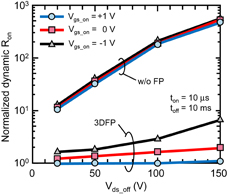
Fig. 16. NDR as a function of off-state drain bias voltage (Vds_off) of reference (without FP) and 3DFP AlGaN/GaN HEMTs with varying on-state gate voltage (Vgs_on).
Download figure:
Standard image High-resolution image
4. Conclusions
With the increasing emphasis for developing highly efficient and "greener" electronic devices, GaN-based electron devices have been generating significant interest in the field of power electronics. In the first half of this paper, after briefly describing the outstanding material properties of GaN and reviewing historical relevant efforts to achieve high breakdown voltages in GaN-based HEMTs, experimental results were presented for pushing the lateral breakdown field toward its theoretical limit. Systematically performed series of experiments on AlGaN/GaN HEMTs, fabricated on a free-standing semi-insulating GaN substrate, identified that parasitic leakage paths responsible for premature device breakdown were likely due to the insufficient structural and electrical quality of GaN buffer layers and the GaN substrate itself. The preparation of a highly resistive semi-insulating GaN substrate, which was realized through carrier compensation by heavy Fe doping (9 × 1019 cm−3), resulted in an effective lateral breakdown field of 2 MV/cm along with a lateral breakdown voltage of 5 kV. This was the highest lateral breakdown field ever reported from any lateral GaN structures. The second half of the paper was devoted to describing various issues relevant to current collapse in AlGaN/GaN HEMTs. Those included experimental procedures to measure current collapse, derivation of formulae to express normalized dynamic Ron (NDR) as a measure of the degree of current collapse, and various experimental attempts to reduce current collapse. By fitting measured NDR curves with a sum of pure exponential terms, important information on the relevant trap states was extracted. The successful combination of two different schemes for intensifying the mitigation effect against current collapse was demonstrated. Finally, a novel device with a 3DFP was shown to exhibit a negligible increase in the dynamic Ron even after being subjected to an off-state drain voltage of 150 V, suggesting that this device may hold the key for true collapse-free operation.
Acknowledgements
This work was partially supported by Grant-in-Aid for Scientific Research (C) (No. 25420328) from JSPS and by a Super Cluster Program from JST. This work was also supported by the Council for Science, Technology and Innovation (CSTI), Cross-ministerial Strategic Innovation Promotion Program (SIP), "Next-generation power electronics" (funding agency: NEDO). The authors would like to thank Professor Kazuyuki Tadatomo, Yamaguchi University, for providing highly resistive GaN substrates. Contributions by Yoshiki Sakaida, Jie Hong Ng, Satoshi Yoshida, and Atsuya Suzuki are also appreciated.
Biographies

Masaaki Kuzuhara received his B.S., M.S., and Ph.D. degrees in electrical engineering from Kyoto University, Kyoto, Japan, in 1979, 1981, and 1991, respectively. He was a Visiting Researcher with the University of Illinois at Urbana-Champaign, IL, USA, from 1987 to 1988. He is currently a Professor with the Department of Electrical and Electronics Engineering, University of Fukui, Fukui, Japan, where he is focusing on physics and characterization of GaN-based heterojunction devices.

Joel T. Asubar received his M.S. and Ph.D. degrees from Nagaoka University of Technology, Niigata, Japan, working on ferromagnetic semiconductors. In 2010, he joined the Research Center for Integrated Quantum Electronics (RCIQE) of the Hokkaido University as a Post-doctoral fellow. Since 2014, he has been a Senior Assistant Professor with the University of Fukui, Fukui, Japan. His research interests include growth of heterojunctions and device physics of GaN-based transistors.

Hirokuni Tokuda received the Ph.D. degree in electronics engineering from the University of Tokyo, Tokyo, Japan, in 1978. He joined Murata Manufacturing Company, Ltd., Kyoto, Japan, in 2002, where he was the General Manager of the Department of Antenna Products. Since 2009, he has been with the University of Fukui, Fukui, Japan. His research interests include GaN-based HEMT devices and their physics.