
Abstract
The photovoltaic industry is in a phase of rapid expansion, growing by more than 30% per annum over the last few decades. Almost all commercial solar cells presently use single-crystalline or multicrystalline silicon wafers similar to those used in microelectronics; meanwhile, thin-film compounds and alloy solar cells are currently under development. The laboratory performance of these cells, at 26% solar energy conversion efficiency, is now approaching thermodynamic limits, with the challenge being to incorporate these improvements into low-cost commercial products. Improvements in the optical design of cells, particularly in their ability to trap weakly absorbed light, have also led to increasing interest in thin-film cells based on polycrystalline silicon; these cells have advantages over other thin-film photovoltaic candidates. This paper provides an overview of silicon-based solar cell research, especially the development of silicon wafers for solar cells, from the viewpoint of growing both single-crystalline and multicrystalline wafers.
Export citation and abstract BibTeX RIS
1. Introduction
Photovoltaic (PV) are promising candidates for future energy sources. The laboratory performance of the solar cells has reached at 26% solar energy conversion efficiency.1) Many countries, including Japan, Germany, The Netherlands, Italy, Switzerland, Spain, and the U.S.A., have programs underway aimed at increasing the use of PV cells, thereby reducing their cost. The most effective recent programs are designed to encourage the urban residential use of PV cells. For example, the total installed peak PV cell capacity in selected countries increased from 1997 to 2008 as shown in Fig. 1.2) The electricity grid essentially provides free storage for the electricity by buying back surplus electricity generated by PVs.

Fig. 1. Total installed peak PV cell capacity in selected countries from 1997 to 2008.
Download figure:
Standard image High-resolution imageMost systems use cells fabricated using silicon wafers with a thickness of approximately 0.2 mm, which is about one-third of the thickness of those used in the microelectronics industry. These wafers are sliced from crystals grown either by the Czochralski (CZ)3) crystal growth technique used in the microelectronics industry or from much larger ingots prepared by directional solidification (DS)4) techniques that result in multicrystalline silicon.
The reduced requirements for material perfection compared with the microelectronics of large-scale integrated circuits (LSIs) means that an off-specification material prepared for the latter industry is used as relatively inexpensive feedstock for these crystal growth processes. The first silicon solar cells were made at Bell Laboratories in the 1940s5) and were partly responsible for the interest in silicon and germanium that led to the explosion of the semiconductor industry in the 1950s.6) A recent burst of activity has led to a 25% increase in the solar energy conversion efficiency, which is close to the fundamental limit of 29% for silicon.7) Further advances in PV cells are required to improve the quality of our lives as well as to reduce energy production costs. Single-crystalline silicon, having already been widely used in solar cells, remains one of the key materials to realize these goals because of its low cost and high quality for energy production. Achieving these improvements requires the low-cost growth of silicon crystals with an even lower concentration of impurities, including oxygen, carbon, and heavy metals, dislocations, and point defects.
The CZ process is a well-established technique for the large-scale production of silicon single crystals for PV cells as well as for LSIs. PV cells based on CZ silicon exhibit a high conversion efficiency, and their production costs are relatively low. The DS process is almost exclusively used for growing silicon ingots for PV applications. The production cost of such silicon materials is even lower than that of CZ silicon; however, the efficiencies of the PV cells are usually lower than those of PV cells based on CZ silicon.8) One of the main impurities, oxygen, is a component of the quartz crucible in which the silicon raw material is melted in both crystal growth methods. The other main impurity is carbon, which acts as a nucleation center for oxygen precipitates, which degrade the lifetime of carriers.9)
The DS and CZ growth methods, as well as the floating zone method, have similar mechanisms of carbon and oxygen incorporation during growth.10) However, because of the specific configurations of the DS growth furnaces, where the quartz crucible is coated with a silicon nitride layer, the concentration of oxygen in crystals grown by the DS method is almost one order of magnitude smaller than that in crystals grown by the CZ method.
Effective control of the oxygen and carbon concentrations is a critical issue for the production of high-quality crystals. Experimental approaches to solving this problem are limited by the time, cost, and complexity of the involved analyses. Developments in computer technologies enable us to find a solution using numerical simulations of the global environments of crystal growth. The main point in the simulation of the impurity contamination processes during crystal growth is the transport of impurities such as oxygen and carbon from their sources to the crystal through the melt. Many simulations of impurity transport have been reported.11–22) Some of these previous investigations included only local simulations11–17) that neglected the mass transport of the impurities in the gas phase. In other cases, the reported simulations included results of global simulations,18–21) some of which only neglected mass transport of oxygen and carbon in the melt,18) whereas others neglected carbon transfer for both the gas and the silicon melt.19–21) The literature contains no reports of simulations that account for both the oxygen and carbon impurities in both the gas and the silicon melt.
Contamination with light elements during the DS process is governed by the mass transport of impurities22) similar in that of the CZ method. Carbon is one of the major impurities in multicrystalline silicon ingots, and it affects the density and electrical activity of dislocations.23) Carbon precipitates to form silicon carbide (SiC) particles when the concentration of carbon exceeds its solubility limit in silicon. These precipitates cause severe ohmic shunts in PV cells.24) Significant degradation of the conversion efficiency in PV cells is due to carbon, oxygen, and SiC particles in a solidified silicon ingot. Carbon will markedly influence the precipitation of oxygen during the thermal annealing of crystals if its concentration exceeds 4 × 10¹⁶ atoms/cm3, which is the solubility limit of carbon in molten silicon.25–30) Oxygen precipitates have been known to act as intrinsic gettering sites for heavy-metal impurities, affecting the mechanical strength of wafers.31,32) Therefore, effective control of the carbon concentration as well as the oxygen concentration in a crystal is required for the production of high-quality crystals.
Contamination by heavy metals such as iron, copper, and nickel is also harmful for improving the conversion efficiency of PV cells. Many experiments and simulations on the contamination of heavy metals have been reported so far.33–37)
Many experiments17,38–41) and numerical simulations42–45) intended to improve the purity of grown crystals have been reported thus far. The carbon and oxygen concentrations in multicrystalline silicon crystals can be affected by a specially designed gas flow system.41) In one reported approach, a tungsten crucible cover in a DS furnace was used to reduce the carbon concentration to a reasonable value; it markedly reduced the O concentration, and the silicon vapor strongly reacted with tungsten.39) Therefore, covers made of SiC-coated carbon are usually used.
Dislocations in crystalline silicon are usually formed during high-temperature crystal growth. The crystal growth process usually contributes to the increase in dislocation density, whereas the cooling process strongly affects the number of dislocations.46) Hence, many studies have focused on the cooling process.47–50) However, the results of these studies are not consistent with each other. Slow cooling was suggested as a means of achieving a low dislocation density in GaP/Si heterostructures47) and in SiGe layers grown via liquid-phase epitaxy.48) By contrast, fast cooling was suggested as a means of achieving a low dislocation density in Pb49) and silicon crystals50) grown from melts. This inconsistency demonstrates that the effect of the cooling process on the dislocation density is complex and differs for different materials, growth furnaces, and growth processes. Clarifying the relationship between the cooling rate and the distribution of the dislocation density requires studies of the effect of the cooling process on the increase in dislocation density with accurate control of the temperature variations inside a furnace according to a predesigned curve. Because the temperature variations inside the furnace have been predesigned, the heater power must be automatically adjusted. This condition can be realized via an automatic control technique such as proportional-integral-differential (PID) control. A numerical solver that simulates an automatic control process has been developed for accurately controlling the temperature variations inside furnaces. Further information on the numerical simulation of the impurities and defects has been reported elsewhere.51)
This review paper surveys methods for improving the conversion efficiency of PV cells by controlling the quality of the crystalline silicon grown by the CZ and DS methods. The main focus of this paper is controlling the concentration of oxygen and carbon impurities in silicon crystals grown by the CZ and DS methods to increase the lifetime of carriers, which directly affect the conversion efficiency of PV cells. This paper also introduces the effect of the cooling process on dislocation multiplication.
2. Numerical results
2.1. Light-element transfer in CZ and DS furnaces
The contamination of silicon ingots with oxygen impurities during both CZ and DS growth is well understood to originate from the dissolution of the silica (SiO2) crucible.42) A typical configuration of a CZ furnace and the argon gas flow rates in the furnace are shown in Fig. 2. Figure 3 shows temperature contours inside the CZ furnace (spacing: 75 K). The oxygen atoms dissolved from the crucible combine with the silicon atoms in the melt to form gas-phase silicon monoxide (SiO) at the gas/melt interface. The SiO is then transferred by the argon gas flow to all of the graphite components in the furnace, reacting with them to form carbon monoxide (CO). The formed CO is then transported back to the silicon melt surface by diffusion and/or convection. Finally, the CO is dissolved into the melt, and carbon and oxygen are segregated into the crystal.

Fig. 2. Configuration of furnace and flow rates in furnace. Reprinted with permission from Ref. 51. © 2015 Springer Japan.
Download figure:
Standard image High-resolution image
Fig. 3. Temperature contours inside CZ furnace (spacing: 75 K). Reprinted with permission from Ref. 51. © 2015 Springer Japan.
Download figure:
Standard image High-resolution imageThe global process of carbon and oxygen transfer is described by the following set of differential equations:


where cSiO, cCO, and cAr are the concentrations of SiO, CO, and argon gas, respectively. The vector uAr is the flow vector of the argon gas. DSiO and DCO in Eqs. (1) and (2) are the diffusivities of SiO and CO, respectively. The gas reaction between SiO and CO was neglected in this study for simplification. The concentrations of the oxygen and carbon atoms in the melt were modeled using the following equations:
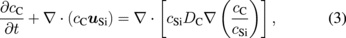
where cC, cO, and cSi are the concentrations of carbon, oxygen, and silicon, respectively, and uSi is the flow vector of the silicon melt. DO and DC are the diffusivities of oxygen and carbon in the melt, respectively, both of which are assumed to be 5.0 × 10⁻⁸ m2/s.44)
The chemistry of the reaction process is the last point to be examined. To complete the model of the process starting from the dissolution of the quartz crucible in the silicon melt, we use the following reaction:

where the index symbols (s), (m), (g), (l), and (c) denote solid, melt, gas, liquid, and crystal, respectively. The oxygen in the melt is transported to the melt–gas interface by convection and/or diffusion, where it reacts with silicon to form SiO:

When SiO(g) comes in contact with the hot carbon embedded in the crucible during the gas-phase transport, the following reaction occurs:

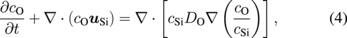
The concentrations of SiO(g) and CO(g) are shown in Figs. 4(a) and 4(b), respectively. The concentration of SiO(g) in the gas was on the order of 10−9 mol/cm3 with a maximum concentration of approximately 7.7 × 10⁻⁹ mol/cm3. The concentration of SiO(g) was high in the center of the furnace and low at the top and bottom because SiO(g) evaporated from the melt surface of silicon and was transferred by the gas from the center of the furnace to the bottom of the furnace. During transport in the furnace, the SiO(g) reacted with the hot carbon walls, and its concentration was gradually reduced. The maximum CO concentration shown in Fig. 4(b) is approximately 6.0 × 10⁻¹⁰ mol/cm3, which occurred at the furnace corners formed by the heat shields labeled 10 and 12 in Fig. 2. This value was one order of magnitude lower than the maximum SiO concentration. The minimum CO concentration was approximately 1.3 × 10⁻¹⁰ mol/cm3, which corresponds to that on the melt surface and that at the top of the furnace. Similar to the distribution of SiO(g), the concentration of CO was high in the center of the furnace, except for inside the crucible.
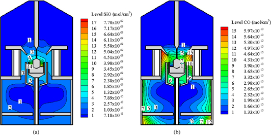
Fig. 4. (a) SiO and (b) CO concentrations in argon gas in the furnace. Reprinted with permission from Ref. 51. © 2015 Springer Japan.
Download figure:
Standard image High-resolution imageThe concentrations of carbon, C(m), and oxygen, O(m), in the melt are shown in Figs. 5(a) and 5(b), respectively. The concentration C(m) in the melt was on the order of 1018 cm−3. The average concentration in the melt was approximately 1.4 × 1018 cm−3. The concentration C(m) in the melt was high at the top of the melt and low at the center of the half-melt. This distribution was consistent with the process where CO(g) was absorbed and dissolved into the melt, followed by the diffusion of carbon into the center of the half-melt. The difference between the distributions of oxygen and carbon is due to the following reasons. Carbon cannot evaporate from the surface of the melt, then the distribution becomes homogeneous. Oxygen evaporates from the surface of the melt during crystal growth. Then, the distribution becomes more inhomogeneous than that of carbon.

Fig. 5. (a) Carbon and (b) oxygen concentrations in the silicon melt. Reprinted with permission from Ref. 51. © 2015 Springer Japan.
Download figure:
Standard image High-resolution imageThis process is basically the same as that of the DS system. Figure 6 shows a typical temperature distribution in a DS furnace. At high temperatures, the silica crucible was partially dissolved into the melt. The dissolved oxygen atoms were then transported to the gas/melt interface and subsequently evaporated as SiO vapor. Subsequently, the SiO was carried by the argon gas flow to all of the graphite components, reacting with them to produce gas-phase CO. The reacted CO was then transported back to the surface of the melt by diffusion and/or convection and subsequently dissolved into the melt. Finally, the C and O atoms were segregated into the crystal lattice. The concentrations of CO and SiO in the furnace are shown in Figs. 7(a) and 7(b), respectively. The concentrations of C and O in the melt are shown in Figs. 8(a) and 8(b), respectively. Their distributions were similar to those in the CZ furnace.
Fig. 6. Temperature contours in DS furnace (spacing: 54 K). Reprinted with permission from Ref. 58. © 2011 Elsevier B.V.
Download figure:
Standard image High-resolution image
Fig. 7. (a) CO and (b) SiO concentrations in furnace. Reprinted with permission from Ref. 58. © 2011 Elsevier B.V.
Download figure:
Standard image High-resolution image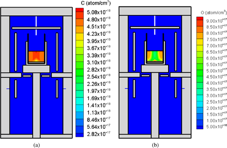
Fig. 8. (a) Carbon and (b) oxygen concentrations in the melt. Reprinted with permission from Ref. 58. © 2011 Elsevier B.V.
Download figure:
Standard image High-resolution imageNitrogen is one of the important impurities in silicon ingots grown by the DS method since silicon nitride is used for the coating of the quartz crucible to prevent the reaction between the silicon melt and the quartz crucible. Nitrogen is dissolved from the coating to the melt, causing precipitation of silicon nitride during crystal growth due to the supersaturation of nitrogen by segregation.52) Details were reported elsewhere which were obtained by numerical calculation with consideration of the phase diagram.53)
To prevent such contamination, we should control the chemical reaction among silicon and other impurities from the beginning of the melting process of the raw materials to the end of the cooling process.54)
2.2. Analysis of dislocation density in silicon crystals
In most reported works concerning the dislocation density in silicon crystals,55–57) thermal stress is regarded as the main cause of dislocations because it drives the multiplication of dislocations in crystals. However, dislocation multiplication and dislocation nucleation are completely different phenomena. Dislocation nucleation is directly related to thermal stress because the nucleation of dislocations requires a stress on the order of the shear modulus of the material (i.e., on the order of GPa), which is impossible to achieve through thermal stress alone during crystal growth and annealing processes. The nucleation of dislocations can only be triggered by a large local stress, possibly caused by factors such as the agglomeration of point defects; surface damage due to the indentation, scratching, grinding, and impingement of hard particles; the presence of a second phase in the form of foreign particles or precipitates; and chemical inhomogeneity due to doping or impurity atoms.57)
The dislocation multiplication driven by the thermal stress determines the final dislocations in the as-grown crystal. The thermal stress is one of the most important factors in determining the presence of final dislocations. To model the dislocation multiplication due to thermal stress, one of two approaches is usually adopted on the basis of whether the crystal is assumed to be elastic or viscoplastic. For an elastic crystal, an elastic problem is solved, and the results yield information about displacements, thermal and elastic strain, and elastic stress inside the crystal. The obtained elastic stress is used to estimate the plastic deformation and whether a particular area of the crystal will have a high or low dislocation density.55) Jordan et al.55) assumed that plastic deformation occurs if the resolved elastic shear stress on any slip system exceeds a critical value, called the critical resolved shear stress (CRSS). For the viscoplastic model, a direct simulation of the time evolution of the dislocation density during the whole crystal growth process is performed; this simulation includes stress relaxation and strain hardening by generated dislocations. The advantage of this approach is that the final dislocation density and the state of the as-grown crystal are functions of the initial conditions of the crystal and the entire growth and cooling temperature histories.45) This approach can also be used to estimate the residual stress in a cooled crystal. A viscoplastic model called the Haasen–Alexander–Sumino (HAS) model is introduced. This model includes a multislip system for the multiplication of dislocations, the immobilization of mobile dislocations, jog formation between different slip systems and its influence on dislocation generation, and the internal stress due to short-range interactions with the total dislocation density. The formulations are given as follows:
First, the force equilibrium should satisfy

where  is the stress tensor. The stress tensor is determined by the constitutive relation

where C and  are the elastic modulus and the elastic strain tensor, respectively. The elastic strain tensor is obtained from

where  ,
,  , and
, and  are the total, plastic, and thermal strain tensors, respectively. The plastic strain is given by the Orowan relationship:56)

where the subscript m denotes a mobile dislocation, the superscript α denotes the slip direction, b is the Burgers vector, N is the dislocation density, and v is the slip velocity of dislocations.
The rate of the mobile dislocation density,  , in slip direction α is given by
where τeff is the effective stress for dislocation multiplication, K and K* are multiplication constants, and rc is the effective dipole half-width. The value of fαβ is either 1 or 0, depending on whether a jog is formed on a screw dislocation of slip system α when cut by a forest dislocation of slip system β. On the right side of Eq. (12), the first term represents the increase in the number of dislocations because of the glide on the slip plane. The second term represents the formation of jogs on a screw dislocation and the consequent expansion through spiral formation, and the third term represents a sink for a mobile dislocation. The slip velocity of a dislocation, v, is given by
where v0 = 5000 m/s, τ0 = 1 MPa, m = 1, and U = 2.2 eV are used for crystalline silicon. The values of K, K*, and rc have been reported elsewhere to be as follows:57)


The effective stress necessary for dislocation motion is given by

where τ(α) is the resolved shear stress,  is the stress required to overcome short-range obstacles, and
  is the internal long-range elastic stress generated by mobile dislocations.57) The value of 〈x〉 is x if x > 0, and it is equal to 0 if x ≤ 0. Details are expressed in Ref. 57.
To confirm the effect of the cooling rate on the generation of dislocations, we used a basic configuration of a unidirectional solidification furnace.58–60) The configuration near the crucible is shown in Fig. 9(a). The crystal growth direction, i.e., the axial line direction, was set to be the [001] direction. The diameter of the cylindrical crystal was 10.6 cm. Both top and side heaters were used. The power ratio of the side heater to the top heater was  . For the numerical simulations, two cooling rates were set, as shown in Fig. 9(b): fast cooling with a ramp rate of 4.7 kW/h in total power and slow cooling with a ramp rate of 1.2 kW/h in total power. The temperature history at a monitoring point (P) is shown in Fig. 9(c). As evident in Figs. 9(b) and 9(c), the temperature history is similar to that of the heater power. Therefore, the present furnace has low thermal inertia, which is helpful for controlling the growth and cooling processes.
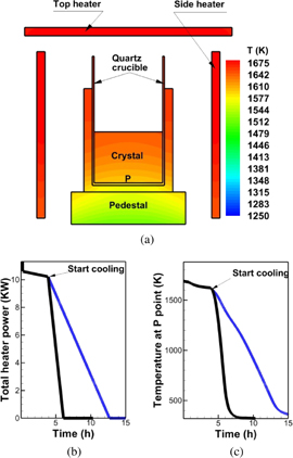
Fig. 9. Furnace structure and cooling settings after crystallization: (a) configuration of furnace near crucible, (b) history of total heater power, and (c) temperature history of point P at bottom of crystal.
Download figure:
Standard image High-resolution imageThe distributions of the dislocation density inside the grown crystal at room temperature for fast and slow cooling are shown in Fig. 10, where Figs. 10(a) and 10(b) show the distributions for the fast and slow cooling rates, respectively. Both cases show inhomogeneous distributions along the cylindrical surfaces. However, at the cylindrical surface under slow cooling, the dislocation density is less than that under fast cooling. Therefore, the cooling rate affects the generation of dislocations during the cooling process. Because the distribution of the final dislocations determines the residual stress inside the grown crystal at room temperature, the cooling rate can conceivably also affect the residual stress. Given that the residual stress inside the crystal is three-dimensional, an average along the peripheral direction was taken; the average residual stresses for the fast and slow cooling rates are shown in Fig. 11, where Figs. 11(a) and 11(b) show fast and slow cooling rates, respectively. The fast cooling rate causes a much higher residual stress inside the crystal. Therefore, the slow cooling rate is beneficial for reducing residual stress.
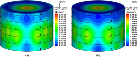
Fig. 10. Distribution of dislocation density in grown crystal at room temperature for [001] growth: (a) fast cooling rate and (b) slow cooling rate.
Download figure:
Standard image High-resolution image
Download figure:
Standard image High-resolution image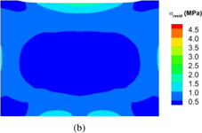
Fig. 11. Distribution of average residual stress in crystal at room temperature for [001] growth: (a) fast cooling rate and (b) slow cooling rate.
Download figure:
Standard image High-resolution image3. Experimental results for controlling oxygen and carbon concentrations in DS and CZ furnaces
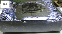
A 50 × 50 × 10 cm3 monolithic Si ingot was grown using a furnace modified for the single-seed cast method, as shown in Fig. 12(a). A quartz crucible with dimensions of 54 × 54 × 43 cm3 was coated with Si3N4. A seed crystal, i.e., a (100) CZ Si crystal with a diameter of 20 cm and thickness of 2 cm, was placed at the center of the crucible. Silicon feedstock (60 kg) was charged to grow a crystal with a height of 10 cm. Boron was used as a dopant to obtain a crystal with a resistivity of 1 Ω cm. Argon gas was flowed to prevent the contamination of O and C from SiO and CO gases during the growth process.61) Two different gas-flow conditions, 10 and 80 l/min, were used. After the crucible was placed inside the furnace, the silicon raw material was heated to 1550 °C to melt the feedstock while maintaining the integrity of the seed crystal. Crystal growth was then started, as shown in Fig. 12(b). Solidification was initiated under special applied thermal conditions and proceeded with a mushroom-shaped interface.62–65)

Fig. 12. (a) Photograph of single-seed cast furnace and (b) schematic of "mushroom" growth.
Download figure:
Standard image High-resolution imageThe grown crystal was cut into several blocks and then sliced into several 2-mm-thick plates. The crystals were characterized by Secco etching to measure the dislocation density. Then, Fourier transform infrared (FT-IR) spectroscopy was used to detect the concentrations of substitutional C [Cs] and interstitial O [Oi] at room temperature. The block was also sliced into a 156 × 156 mm2 wafer for the measurement of the carrier lifetime and the conversion efficiency of the crystals. For comparison, a CZ Si wafer was processed as a reference sample. The lifetime of the wafer was increased from 122 to 465 µs by increasing the height of the ingot from 20 to 90 mm. The values were measured by the microwave photo-conductance decay method (micro-PCD) after a gettering process. The cell efficiency also increased from 9.2 to 18.7% with increasing height of the ingot. The values were almost identical to those obtained by CZ wafers.
Figure 13 shows the ingot grown by the single-seed cast method. The surface is shiny and free from impurity precipitates. The multiple crystals grown by the conventional method do not exhibit a mirror-like surface, as shown in Figs. 13(a) and 13(b). Figure 13(b) shows a habit structure, which is evidence of a low density of dislocations. Figure 14 shows the variation of the etch pit density (EPD) as a function of the height of the ingot. The EPD at the seed was approximately 2 × 104 cm−2 and decreased to 3 × 103 cm−2 with increasing height of the ingot.
Download figure:
Standard image High-resolution image
Fig. 13. Photographs of (a) conventional cast multicrystalline silicon ingot and (b) its top surface.
Download figure:
Standard image High-resolution image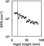
Fig. 14. Variation of EPD of single-seed cast ingot.
Download figure:
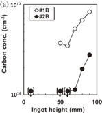
Standard image High-resolution imageFigure 15 shows the concentrations of C and O as functions of the ingot height. The two crystals labeled #1B and #2B were grown in a furnace under conditions involving two different gas velocities: 50 and 100 l/min. The concentration of C in both #1B and #2B increases with the ingot height, although the C concentration in #2B is approximately three times smaller than that in #1B, as shown in Fig. 15(a). By contrast, the concentration of O decreases with increasing height, as shown in Fig. 15(b), and the O concentrations of #1B and #2B do not substantially differ from each other. These data indicate that a large argon flow contributes to the reduction of the concentration of C in a crystal. The decrease in the oxygen concentration with increasing crystal height can be explained by the evaporation of oxygen from the surface of the melt during crystal growth. The increase in the carbon concentration with the height is due to the accumulation of carbon in the melt by segregation, and carbon is a nonvolatile impurity.
Download figure:
Standard image High-resolution image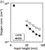
Fig. 15. Variation of (a) substitute C and (b) interstitial O concentrations with ingot height for different argon gas-flow velocities: #1 (50 l/min) and #2 (100 l/min).
Download figure:
Standard image High-resolution image
4. Conclusions
With the aid of computer simulations of the global environments of crystal growth techniques, technical solutions that improve the purity of the crystals can be identified. The behavior of oxygen and carbon impurities, which are the main light-element impurities in silicon crystals, can be well described by simulations of heat and mass transfers in a CZ furnace. The models can be applied in the same manner to the unidirectional solidification process.
To improve the conversion efficiency, we have to encourage research and development on improvement of the carrier lifetime. We need to understand and control the formation mechanism of thermal donor and oxygen precipitates including point defects to achieve this improvement.66)
Acknowledgment
This work was partly supported by MEXT/JSPS KAKENHI Grant Number 15K13351.
Biographies

Koichi Kakimoto is Professor of the Institute of Applied Mechanics of Kyushu University. He received his Ph.D. in Engineering in 1985 from the Graduate School of Electronic Engineering, University of Tokyo. Previous positions included Researcher of NEC Fundamental Research Laboratories (1985), Visiting Researcher of Universite Catholique des Louvain in Belgium (1989), Visiting Professor of Institute of Materials Research (KINKEN) of Tohoku University (1995). His research focuses on the effects of external fields on melt flow and crystallization. He is a president of International Organization for Crystal Growth.

Bing Gao is project associate professor of the Institute of Applied Mechanics of Kyushu University. He received his Ph.D. in Engineering in 2008 from Korean Advanced Institute of Science and Technology. He received Goesele young researcher award in 2015. His research focuses on dislocation analysis and crystallization.

Satoshi Nakano is a technical staff of Institute of Applied Mechanics of Kyushu University. He received his Ph.D. in Engineering in 2012 from Kyushu University. His research focuses on crystal growth of semiconductors.

Hirofumi Harada is a research fellow of Institute of Applied Mechanics of Kyushu University. He received his Ph.D. in Science in 1980 from Tohoku University. His research focuses on crystal growth and dislocation analysis of semiconductors.

Yoshiji Miyamura is a research fellow of Institute of Applied Mechanics of Kyushu University. He received his Ph.D. in Science in 2015 from Tsukuba University. His research focuses on crystal growth and CVS of semiconductors.