

Abstract
We have achieved a record high cell efficiency of 20.29% for an industrial 6-in. p-type monocrystalline silicon solar cell with a full-area aluminum back surface field (Al-BSF) by simply modifying the cell structure and optimizing the process with the existing cell production line. The cell efficiency was independently confirmed by the Solar Energy Research Institute of Singapore (SERIS). To increase the cell efficiency, for example, in four busbars, double printing, a lightly doped emitter with a sheet resistance of 90 to 100 Ω/□, and front surface passivation by using silicon oxynitride (SiON) on top of a silicon nitride (SiNx) antireflection layer were adopted. To optimize front side processing, PC1D simulation was carried out prior to cell fabrication. The resulting efficiency gain is 0.64% compared with that in the reference cells with three busbars, a single antireflection coating layer, and a low-sheet-resistance emitter.
Export citation and abstract BibTeX RIS
1. Introduction
Reducing processing cost is a major goal for today's solar industry not only for lowering economical risks but also for obtaining a higher gross margin. A key driver of cell processing cost per watt peak is the efficiency of the cell in obtaining as much power out of the solar cells as possible.1–5) Assuming that all other things are equal, a 1% point increase in cell efficiency reduces cell cost by about 6%.6) If a cell producer increases the cell efficiency relatively more than the additional cost required to achieve the efficiency gain, the producer decreases the cost per watt.
Screen printing is the mainstream technology, and a current trend in metallization related to the number of busbars (BBs) is expected, that is three BBs, still dominating today, will be replaced by four and/or five BBs.7) We have reached a cell efficiency record of 20.29% for an Al-BSF solar cell, and the solar cell was fabricated on a 6-in. industrial boron-doped Czochralski (Cz) Si substrate with conventional cell processing optimization without the extra cost and additional cell manufacturing equipment. The cell efficiency of 20.29% was confirmed by the Solar Energy Research Institute of Singapore (SERIS). To increase the cell efficiency as well as to decrease the production cost, we have developed competitive Al-BSF cell technology using conventional cell manufacturing technology without the selective emitter already reported in 2012.8)
To improve the cell processing, we have adopted four BBs, double printing,9–14) a lightly doped emitter, and front surface passivation by using silicon oxynitride (SiON) on top of an antireflection layer. To optimize front-side processing, PC1D simulation was carried out prior to cell fabrication.15–23) Through PC1D simulation, we have estimated the peak doping depth of the emitter, which was confirmed by electrochemical capacitance–voltage (ECV) measurement. Finger number and width were also estimated.
2. Experimental methods
To improve cell processing, PC1D simulations were carried out; here, we have set a reference cell with three BBs, single printed fingers, emitter sheet resistances of 75 to 85 Ω/□, and silicon nitride (SiNx) single antireflectance layer for comparison. The reference cell efficiency starts at 19.65%. Solar cells were fabricated on 6-in. industrial boron-doped Cz-Si substrates, 180 µm thick, 〈100〉-oriented, and 1.5–3 Ω cm, by conventional cell processing. The wafers were textured with alkaline solution for 3–5-µm-sized pyramid formation, and then doped with phosphorous oxychloride (POCl3) using a diffusion furnace at a temperature lower than 900 °C. The emitter sheet resistance was varied according to the simulation results. After phosphorus silicate glass (PSG) removal and the wet isolation of the rear side, dual antireflection layers (SiNx/SiON) were deposited successively on top of the emitter by plasma-enhanced chemical vapor deposition (PECVD) in a direct plasma system operating at a radio frequency (RF) of 13.56 MHz. A mixture of reactant gases, such as silane (SiH4), nitrous oxide (N2O), and ammonia (NH3) was used for the deposition of the SiON layer. For the SiNx layer deposition, we used the reactant gases SiH4 and NH3. Both the PECVD processes used for the deposition of the dual antireflection layer stack were realized without breaking the vacuum. All samples were screen printed and cofired to form both side electrodes.24–28)
To characterize the cells, quantum efficiency, reflectance, and current–voltage (I–V) measurements were carried out. The best cell efficiency was confirmed by SERIS.
3. Results and discussion
To optimize the cell process, we carried out PC1D simulation prior to cell fabrication. For reference, we fitted the simulation results to the output characteristics of the cells from our cell production line. Our reference cell consists of three BBs, single-printed fingers, and silicon nitride (SiNx) as an antireflection layer. The efficiency of the reference cell is 19.65%. The most important simulation conditions for each simulation group defined by cell efficiency are listed in Table I. The effects of dual passivation layers (groups 1 and 2), finger aspect ratio (groups 3 to 6), and peak doping depth (groups 7 to 9) were simulated by keeping all the other parameters constant. Through the simulation, for each number of BBs, the optimum number and width, i.e., aspect ratios of fingers were determined. The simulation was performed with the input parameters shown in Table II, where the series resistance (Rs) and optical loss were calculated with the equations given by Mette and Burgers.29,30)
Table I. Results of the PC1D simulation (finger width: 50 µm for groups 1 to 3; 45 and 40 µm for groups 4 and 5, respectively; 35 µm for Groups 6 to 9).
| Group | Voc (mV) | Jsc (mA/cm2) | FF (%) | η (%) | Rs (mΩ) | Opt. loss (%) | |
|---|---|---|---|---|---|---|---|
| 1 | 3BB, SP, SiNx | 641.6 | 38.38 | 79.83 | 19.65 | 2.47 | 7.10 |
| 2 | 3BB, SP, SiNx/SiON | 641.9 | 38.79 | 79.68 | 19.84 | 2.47 | 6.10 |
| 3 | 3BB, DP, SiNx/SiON | 641.9 | 38.79 | 79.91 | 19.90 | 2.31 | 6.10 |
| 4 | 3BB, DP, SiNx/SiON | 641.9 | 38.79 | 80.07 | 19.94 | 2.20 | 6.10 |
| 5 | 3BB, DP, SiNx/SiON | 641.9 | 38.81 | 80.23 | 19.99 | 2.08 | 6.03 |
| 6 | 3BB, DP, SiNx/SiON | 641.9 | 38.87 | 80.34 | 20.04 | 2.00 | 5.91 |
| 7 | 4BB, DP, SiNx/SiON | 642.0 | 38.92 | 80.67 | 20.15 | 1.76 | 5.78 |
| 8 | 4BB, DP, SiNx/SiON | 642.2 | 38.92 | 80.67 | 20.16 | 1.76 | 5.78 |
| 9 | 4BB, DP, SiNx/SiON | 645.2 | 38.94 | 80.72 | 20.30 | 1.76 | 5.78 |
Table II. Input parameters for the PC1D simulation.
| Base thickness (µm) | 180 |
| Base resistivity (Ω cm) | 1.5–3 |
| Aspect ratio and number of fingers | Variable (%) |
| Finger width (µm) | |
| Groups 1 to 3 | 50 |
| Groups 4 and 5 | 45, 40 |
| Groups 6 to 9 | 35 |
| Number of BBs | Three and four BBs |
| Peak doping depth | Variable (nm) |
| Series resistance Rs (mΩ) | 1.5–3 |
| Optical loss (%) | 5–8 |
In Table I, PC1D simulation results are also presented. In group 2, with dual antireflection layers of SiNx/SiON, the cell efficiency increases by 0.2% with a 1% reduction in optical loss as compared with group 1, where a single antireflection layer is adopted.
By employing the double printing condition in simulation group 3, the fill factor (FF) increases by 0.23% owing to a decrease in series resistance. With double printing, an approximately 0.06% efficiency gain can be obtained as shown in Table I.
In three BB double printing groups 3 to 6, electrical simulations were performed in order to optimize the front-side metallization grid. In these groups, by increasing the number of fingers and decreasing the finger width from 50 to 35 µm while keeping the aspect ratio of fingers constant at double printing (DP), the optimum number of fingers and finger width were simulated. The front electrode design with a certain number of fingers set at 100 to 120 and a finger width of 35 µm in group 6 yields the lowest optical loss and series resistance; thus the group 6 simulation condition was chosen for the next simulation step (group 7).
In group 7, the other parameters were set the same, but four BBs were employed. To improve the cell efficiency, the optical loss caused by shadowing should be reduced while minimizing electrical loss due to an increase in series resistance with narrowing fingers. Optical and electrical losses can be compensated by controlling the finger number and width with a certain finger height.
In group 7 with four BBs, with decreasing optical loss, the short circuit current density (Jsc) increases by 0.33 mA/cm2, resulting in an efficiency gain of 0.11%. For four BB simulation, the BB width was set to about 70% of that for three BB simulation, and the number of fingers was set between 110 and 120.
In four BB groups 7 to 9, the peak doping depth was varied from 5 to 15 nm at constant finger design determined in simulation group 6. When the peak doping depth is 15 nm in group 9, an increase in open circuit voltage (Voc) results in efficiency gains up to 0.15% for our simulation. The process conditions estimated by the simulation were applied to cell processing.
After the simulation, double-printed three and four BB Al-BSF cells were fabricated on 180-µm-thick large-area 6-in. Cz boron-doped silicon wafers with resistivities of 1.5–3 Ω cm. An antireflection coating is an important feature of solar cells. This layer should not only minimize optical reflectance but simultaneously suppress surface recombination. Figure 1 shows the reflectance for the cells with SiNx single antireflection layer and dual layers of SiNx/SiON. The higher passivation and lower reflectance of the cell with dual antireflection layers result in a higher external quantum efficiency as shown in Fig. 2, where the cell with a single antireflection layer was set as a reference for comparison. By using the dual antireflection layers, the short circuit current density is boosted by 0.34 mA/cm2, resulting in efficiency gains up to 0.18%, in comparison with the single antireflection layer cell as shown in Table III. By using the dual antireflection layers, the passivation and light trapping are improved in comparison with a single antireflection layer. To minimize the absorption in SiON, the refractive index (RI) and thickness should be more carefully controlled.31) The total thickness of the dual antireflection layers for our cells is about 100 to 200 nm.

Fig. 1. Wavelength vs reflectance for the cells with single and dual antireflection layers.
Download figure:
Standard image High-resolution image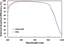
Fig. 2. External quantum efficiency for the cells with single and dual antireflection layers.
Download figure:
Standard image High-resolution imageTable III. Output gains of dual antireflection layers.
| ARC | ΔVoc (mV) | ΔJsc (mA/cm2) | ΔFF (%) | Δη (%) |
|---|---|---|---|---|
| SiNx | 0 | 0 | 0 | 0 |
| SiNx/SiON | +2.2 | +0.34 | 0 | +0.182 |
Figure 3 shows the emitter doping profiles measured by using the ECV technique.32–39) The output gains are shown in Table IV, where "doping 1" was set as a reference. With the deep junction forming the lightly doped emitter, the efficiency gain increases up to 0.13% owing to the Voc increase of 3.9 mV as shown in Table IV. Surface recombination can be reduced while minimizing loss in FF by reducing the surface concentration of dopants and the formation of a deep emitter junction. The FF loss can be compensated by the optimum number of fingers and finger width as estimated by the simulation.

Fig. 3. Doping profiles obtained by ECV measurement.
Download figure:
Standard image High-resolution imageTable IV. Output gains of the cells with different doping conditions.
| Conditions | ΔVoc (mV) | ΔJsc (mA/cm2) | ΔFF (%) | Δη (%) |
|---|---|---|---|---|
| Doping 1 | 0 | 0 | 0 | 0 |
| Doping 2 | +0.8 | +0.237 | −0.261 | +0.069 |
| Doping 3 | +3.9 | +0.184 | −0.320 | +0.133 |
Figure 4 shows the I–V curve of the double printed four BB cell with dual antireflection layers fabricated according to the optimum simulation results. The certified record efficiencies are 20.2 and 20.29% for the three and four BB cells, respectively, as shown in Table V. For our screen printing process, the finger width is less than 40 µm, resulting in not only less shading loss but also less electrical loss at the optimum number of fingers.

Fig. 4. I–V characteristics of four BB double-printed Al-BSF solar cell, which was certified by SERIS.
Download figure:
Standard image High-resolution imageTable V. Output results of the cells certified by SERIS.
| Cells | Voc (mV) | Jsc (mA/cm2) | FF (%) | η (%) |
|---|---|---|---|---|
| Three BBs | 649.4 | 38.84 | 80.09 | 20.20 |
| Four BBs | 647.0 | 38.76 | 80.92 | 20.29 |
For double printing, we have reduced the finger width and increased the finger height at the optimum number of fingers without finger interruption. For the four BB cell, 0.09% efficiency gain was obtained over the three BB cell as shown in Table IV.
Figure 5 shows Shinsung Solar Energy's cell production efficiency for the double printing line. For mass production, the average cell efficiency reached 20.12% for 10,000 runs, with a maximum efficiency of 20.30%, and in most of the runs, it was above 20%.

Fig. 5. Cell production efficiency for double printing line.
Download figure:
Standard image High-resolution image
4. Conclusions
Three and four BB cells with dual antireflection layers were investigated for single and double printing methods. We have achieved a record high cell efficiency of 20.29% for industrial 6-in. p-type monocrystalline silicon Al-BSF solar cells by simply modifying the cell process with the existing cell production line. To improve cell processing, for example in four BBs, double printing, lightly doped emitter, and front surface passivation by using SiON on top of an antireflection layer were adopted. The highest cell efficiency of 20.29% was certified by SERIS. For mass production, the average cell efficiency reached 20.12% for 10,000 runs, with a maximum efficiency of 20.30%, and in most of the runs, it was above 20%. This shows that production cost could be reduced even by conventional cell production with higher efficiency.