

Abstract
Half-Heusler compounds, which possess robust mechanical strength, good high temperature thermal stability and multifaceted physical properties, have been verified as a class of promising thermoelectric materials. During the last two decades, great progress has been made in half-Heusler thermoelectrics. In this review, we summarize some representative work of p-type half-Heusler materials, the thermoelectric performance of which has been remarkably enhanced in recent years. We introduce the features of the crystal and electronic structures of half-Heusler compounds, and successful strategies for optimizing electrical and thermal transport in the p-type RFeSb (R = V, Nb, Ta) and MCoSb (M = Ti, Zr, Hf) based systems, including band engineering, the formation of solid solutions and hierarchical phonon scattering. The outlook for future research directions of half-Heusler thermoelectrics is also presented.
Export citation and abstract BibTeX RIS
1. Introduction
The rapid development of our economy and society is demanding huge energy consumption, which is mainly supplied by non-renewable fossil fuels. However, over 50% of the energy is lost by wasted heat, which can actually be reused [1], and the combustion of fossil fuels also causes severe environmental problems, such as atmospheric pollution and global warming. Thermoelectric (TE) conversion technology, which can convert heat into electricity directly without any emission or vibrational parts, offers a sustainable solution to these problems. In order to expand the application of TE technology, the key challenge is to improve the performance of TE materials, which is represented by the dimensionless figure of merit zT = α2σT/(κe + κL), where α, σ, T, κe and κL are the Seebeck coefficient, electrical conductivity, absolute temperature, and electronic and lattice contributions to the total thermal conductivity κ, respectively.
Benefitting from the development of modern theories, the applications of advanced synthesis and characterization techniques, tremendous exploratory efforts in thermoelectrics have been carried out and continuous breakthroughs have been made in the past few decades [2, 3]. There are many families of TE materials with zT values exceeding unity, some even higher than 2. In near-room temperature application (300–500 K), (Bi, Sb)2(Te, Se)3-based materials still play an important role. With the development of nanostructure engineering [4], dislocation engineering [5], texture engineering [6] and point defects engineering [7], remarkable progress has been made to enhance the TE and mechanical performance of bismuth-telluride-based alloys. Meanwhile, promising MgAgSb-based alloys, with earth-abundant and nontoxic constituent elements, have begun to attract attention because of their high zT values of 1.1–1.4 near 500 K [8, 9]. For medium temperatures (500–900 K), IV–VI compounds, such as PbTe and SnTe and their alloys, are primary materials systems [10–14]. Other environment-friendly compounds such as skutterudites [15, 16], Mg2(Si, Ge, Sn) [17, 18], and Cu2(S, Se, Te) [19, 20], also show potential for medium-temperature application due to their unique structures and attractive TE performance. For high-temperature TE materials (>900 K), traditional and prestigious SiGe alloys have been investigated for more than 50 years [21, 22]. Although a high zT of >1 was reported for nanostructured n-type SiGe [21], the application of these alloys was mainly limited by the poor performance of p-type materials (peak zT ≈ 0.6) [22].
In recent years, half-Heusler (HH) compounds, such as MNiSn, MCoSb (M = Ti, Zr, Hf) and RFeSb (R = V, Nb, Ta), have gained increasing popularity as promising high-temperature TE materials due to their excellent TE properties (zT > 1 for both n-type and p-type materials) [23, 24]. Besides a high zT, the mechanical robustness and thermal stability are also important in determining the applicability of TE materials due to their inevitable exposure to various mechanical and thermal stresses. The outstanding mechanical properties of HH alloys have been reported by Rogl et al [25], compared to those of Bi2Te3 [26] and PbTe [27], and the reproducibility of good TE performance after a long-term annealing process or thermal cycle has also been demonstrated [28–30]. Such advantageous intrinsic properties of HH materials highlight their application potential in high temperature power generation.
The advanced synthesis techniques also promote the study of HH materials. The difficulty in the fabrication of HH compounds mainly lies in the distinct differences in specific gravity and the melting point of constituent elements. Many traditional fabrication methods, such as solid-state synthesis [31], arc-melting [32] and mechanical alloying [33], always call for a long-term annealing process to ensure microstructural and compositional homogeneity. Recently, a time-efficient synthesis process combining levitation melting with spark plasma sintering (SPS) has been reported to prepare high quality HH samples [34, 35]. Some novel methods, such as self-propagating high-temperature synthesis (SHS) [36], chemical reaction [37] and melt spinning [38] combined with SPS, were also applied to synthesize HH materials, opening up more ways for efficient material preparation.
For a long time, the research and progress of HH materials has mainly focused on n-type alloys, especially MNiSn-based alloys. As a typical class of HH materials, the high κ of this system has been the main obstacle to achieving high zT [38]. Therefore, several strategies, such as alloying [39, 40], nanostructuring [41], and phase separation [42], have been adopted to suppress lattice thermal conductivity by enhancing phonon scattering. The high zTs of >1 for n-type HH materials has been achieved, as shown in figure 1(a). However, for a long time, p-type HH materials have exhibited a reproducible maximum zT of only ~0.5 [43–45]. In recent years, remarkable progress has been made in p-type materials, the zT of which is even higher than that of n-type materials (figure 1(b)). Figure 1(c) shows the evolution of peak zT for typical HH materials since 2000. One can see that MCoSb- and RFeSb-based compounds are the two protagonists in the study of p-type HH TE materials, and have gone through a rapid development in the past five years.
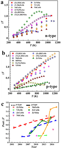
Figure 1. The temperature dependence of zT for typical (a) n-type [40, 42, 48–54] and (b) p-type half-Heusler materials [35, 55–62]. (c) Evolution of the peak zT values for some typical HH materials [28, 33, 35, 42–44, 48, 50, 54, 56, 59, 60, 63–76].
Download figure:
Standard image High-resolution imageThere have been several good reviews on HH TE materials. Xie et al have reviewed the recent advances in nanostructured HH compounds [46]. Chen et al have summarized the synthesis methods for optimizing individual parameters to enhance the TE performance in both MNiSn- and MCoSb-based HH alloys [23]. Zhu et al introduced the application of an advanced fabrication process to HH compounds as well as optimization strategies for MNiSn- and RFeSb-based alloys [24]. More recently, Zeier et al provided an overview of the electronic properties of HH compounds using Zintl chemistry, opening a new perspective to understand their basic structural chemistry and physical properties [47]. All these reviews do not reflect the recent advances in p-type high performance HH materials. Therefore, this review is focused on the p-type RFeSb- and MCoSb-based alloys, especially the relationship between the electronic structure and TE properties and the optimization strategies. Some representative work on p-type RFeSb and MCoSb are listed in table 1 with a time sequence.
Table 1. Representative work of p-type RFeSb and MCoSb with a time sequence. The synthesis methods are expressed as abbreviations, e.g. arc-melting (AM), annealing (AN), ball milling (BM), hot pressing (HP), spark plasma sintering (SPS), mechanical alloying (MA), and levitation melting (LM).
| Composition | Methods | Peak zT (temp.) | Highlights | Reference |
|---|---|---|---|---|
| V0.8Ti0.4FeSb | MA + SPS | 0.43 (773 K) | p-type doping | [68] |
| (V0.6Nb0.4)0.8Ti0.2FeSb | LM + BM + SPS + AN | 0.8 (900 K) | Doping and alloying | [66] |
| Nb0.8Ti0.2FeSb | LM + BM + SPS + AN | 1.1 (1100 K) | Band engineering | [65] |
| Nb0.88Hf0.12FeSb | LM + BM + SPS + AN | 1.47 (1200 K) | Decouple TE transport | [56] |
| Nb0.75Ti0.25Fe1.05Sb | LM + BM + SPS + AN | 1.34 (1150 K) | Hierarchical scattering | [77] |
| (Nb0.6Ta0.4)0.8Ti0.2FeSb | LM + BM + SPS + AN | 1.6 (1200 K) | Ta alloying | [35] |
| Zr0.5Hf0.5CoSb0.8Sn0.2 | AM + AN | 0.5 (1000 K) | Hf alloying | [43] |
| Hf0.44Zr0.44Ti0.12CoSb0.8Sn0.2 | AM + BM + HP | 0.8 (973 K) | Nanostructuring | [58] |
| Zr0.5Hf0.5CoSb0.8Sn0.2/HfO2 | AM + BM + SPS | 0.75 (900 K) | Nano-composite | [78] |
| Ti0.25Hf0.75CoSb0.85Sn0.15 | AM + AN | 1.2 (983 K) | Phase separation | [55] |
| ZrCo1.05Sb0.9Sn0.1 | AM + AN + BM + HP | 0.56 (773 K) | Nano-composite | [79] |
2. Crystal structure of HH compounds
Typical HH compounds are ternary intermetallics with a general formula XYZ, according to the order of element electronegativity. X represents the most electropositive element, which can be a main group element, a transition metal or a rare earth element. Y is usually the less electropositive metal, and the most electronegative element, Z, placed at the end, is usually a main group element from the right half of the periodic table, e.g. ZrNiSn, VFeSb, YPtSb. However, the lattice occupancy cannot be directly derived from the nomenclature. HH compounds generally crystalize in a cubic structure with a space group  . A characteristic feature of this HH structure is three interpenetrating fcc sublattices, each of which is occupied by three kinds of atom, respectively. The corresponding occupied Wyckoff positions are 4a (0, 0, 0), 4b (1/2, 1/2, 1/2), and 4c (1/4, 1/4, 1/4), as shown in figure 2. Generally, the HH structure can be viewed as a ZnS sublattice (Wyckoff positions 4a and 4c), in which the octahedral sites (4b) are occupied. This description emphasizes the covalent bonding interaction between the elements of 4a and 4c, which plays a major role in the electronic properties of the material. In contrast, the atoms at position 4a and 4b build a NaCl-type sublattice, i.e. their interaction has a strong ionic character. Position 4c is unique because switching all the elements on the 4a and 4b positions results in the same, but inverted, structure. However, switching element 4a or 4b with 4c would make a different material. Therefore, it has to be noted that although MgAgAs is always viewed as a prototype of a HH compound in thermoelectrics, it actually crystallizes differently from many reported HH TE materials, such as ZrNiSn, NbFeSb and ZrCoSb, because in MgAgAs, Ag and anionic As form the covalent ZnS-sublattice, while Mg and Ag build the NaCl-type lattice. In contrast, MgCuSb is a better choice to represent the atomic arrangement for most HH materials because the Cu and anionic Sb form the ZnS-sublattice, and the electropositive Mg and electronegative Sb occupy the ionic NaCl-type sublattice [80]. Further details regarding the crystal structure of HH compounds can be found in [47, 80].

Figure 2. Crystal structure of HH compound.
Download figure:
Standard image High-resolution imageGenerally, high performance TE materials are heavily doped semiconductors, and HH materials with 18 valence electrons usually exhibit semiconducting properties. The most attractive properties of HH materials for thermoelectrics are their high Seebeck coefficient up to ~300 µV K−1 at room temperature and their high electrical conductivity (~104 Sm−1). But the simple crystal structure leads to a relatively high thermal conductivity, which can be as high as ~10 W m−1 K−1 [24, 81, 82]. Fortunately, the three occupied fcc sublattices provide possibilities and the flexibility of doping and alloying, which are favorable for enhancing TE performance, and will be discussed in detail in the following sections.
3. Improving electrical transport
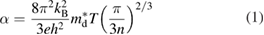
The VFeSb HH compound displays a high negative Seebeck coefficient (approximately –200 µVK−1 at 300 K), and a large power factor (4.5 × 10⁻³ W m−1 K−2 at 300 K), but a relatively high thermal conductivity (10 W m−1 K−1 at 300 K) [34, 53]. Therefore, VFeSb was studied as an n-type TE material in its early years. The strategies for improving the TE performance of VFeSb-based alloys focused on the reduction of lattice thermal conductivity, which only led to a marginal improvement of zT with a maximum value of 0.33 [33, 34, 53, 83], and there have rarely been investigations on the p-type doping and TE properties for this system. However, electronic structure calculations reveal that the band structure of VFeSb is similar to that of ZrCoSb (figure 3), which is usually studied as a p-type TE material. In the band structure, one of the most important parameters is the density of state (DOS) effective mass ( ). For metals or degenerate semiconductors (parabolic band and energy-independent scattering approximation), the Seebeck coefficient is given by [84]:
where n is the carrier concentration, T the abstract temperature, and  is the DOS effective mass.

Figure 3. Band structure of (a) ZrCoSb and (b) VFeSb. We found spin orbital coupling has negligible effect on the band structures.
Download figure:
Standard image High-resolution imageA large  means a large Seebeck coefficient. A large
  can be achieved by either a high band degeneracy (NV) or a heavy single band effective mass
  because
  [85]. As has been mentioned in section 2, a HH compound crystalizes in a cubic structure with space group
  . The high symmetry of a simple HH structure usually leads to a large band degeneracy. Figure 3(a) shows that the conduction band minimum of VFeSb is located at point X with a band degeneracy of NV = 3. In contrast, the valence band maximum (VBM) is located at point L with twofold orbital degeneracy and fourfold valley degeneracy. The high band degeneracy (NV = 8) of the valence band makes VFeSb more promising as a p-type TE material rather than an n-type material.
Zou et al first investigated the TE properties of p-type V0.8Ti0.4FeSb and realized a zT of 0.43 at 773 K [68]. Although the zT of this p-type alloy is higher than that of the n-type counterpart, the high thermal conductivity restrains the TE performance. V and Nb both belong to the VB group. Nb alloying at the V site is expected to decrease the thermal conductivity due to enhanced point defect scattering [83]. Fu et al investigated the TE properties of Nb alloyed (V0.6Nb0.4)1−xTixFeSb, and realized a high zT of 0.8 at 900 K when x = 0.2 (figure 4(a)) [66]. It was one of the highest reported zT values for p-type HH compounds at that time, even higher than the state-of-the-art p-type SiGe alloys (zT ≈ 0.6) for high temperature TE application [86]. Ti acts as p-type dopant and increases the hole concentration in (V0.6Nb0.4)1−xTixFeSb, which leads to a high power factor (figure 4(a)). In addition, the substitution of high content Ti at the V site also increases the point defect scattering and phonon–electron scattering compared to the Co doped n-type (V0.6Nb0.4)1−yCoyFeSb [53], resulting in a more remarkable reduction of lattice thermal conductivity. Figure 4(b) shows the Ti content dependence of κL.
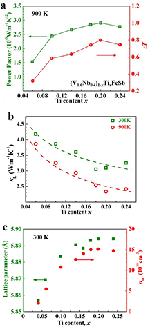
Figure 4. (a) Ti content dependence of power factor (green) and zT (red). [24] John Wiley & Sons. © 2015 WILEY-VCH Verlag GmbH & Co. KGaA, Weinheim. (b) Lattice thermal conductivity for p-type Ti doped (V0.6Nb0.4)1−xTixFeSb HH compounds. The dashed lines show the trend of the experimental data. [66] John Wiley & Sons. © 2014 WILEY-VCH Verlag GmbH & Co. KGaA, Weinheim. (c) Ti content dependence of lattice parameter and carrier concentration. [66] John Wiley & Sons. © 2014 WILEY-VCH Verlag GmbH & Co. KGaA, Weinheim.
Download figure:
Standard image High-resolution imageIt is worth noting the solubility of the dopant in the (V, Nb)FeSb matrix. The lattice parameters and carrier concentrations increase with an increase in Ti content and remain almost unchanged at x ⩾ 0.2 (figure 4(c)), indicating that the solubility limit of Ti has been reached [66]. Impurity peaks can be found in the XRD pattern for 40% Ti-doped NbFeSb [28]. The EPMA results (supporting information in [77]) show that all the Nb0.75Ti0.25Fe1+xSb samples have a similar actual Ti content of ~23%, confirming that the solubility of Ti in NbFeSb is lower than 23%. In the V excess V1.2FeSb matrix, Zou et al reported that V0.8Ti0.4FeSb is phase pure [68]. Ti dopant has similar solubility in a Nb-rich and V-rich matrix, but Zr and Hf, which are the same group IVB element as Ti, have a higher solubility in a Nb-rich matrix than in a V rich matrix [87].
When endeavoring to further enhance the TE performance of p-type Nb alloyed (V0.6Nb0.4)1−xTixFeSb, two issues arise. Firstly, the theoretical optimal carrier concentration cannot be realized due to the solubility limit of the Ti dopant. Secondly, the low mobility µ of (V0.6Nb0.4)1−xTixFeSb should be improved for further zT enhancement. A direct strategy to solve those two issues is to decrease  (or
(or  when NV is fixed). As shown in figure 5(a), the optimal carrier concentration (nopt) is approximately positively correlated to the DOS effective mass
  . A large
  that produces a large Seebeck coefficient, in contrast, will result in a low carrier mobility because the carrier mobility is inversely proportional to the inertial effective mass
  and single band effective mass
  ,
,  assuming that the acoustic phonon scattering dominates the transport [85]. Hence, decreasing
  will have dual effects in improving the electrical properties. Theoretical studies have revealed that the VBMs of VFeSb and NbFeSb are mainly provided by the outer d-orbital of the transitional metal [65, 88, 89]. Due to the relative localization of the d-orbital, the band effective mass of the valence band is always large. The decrease in
  can be realized by substituting more Nb at the V site because the 4d orbital of Nb is less spatially localized than the 3d orbital of V.
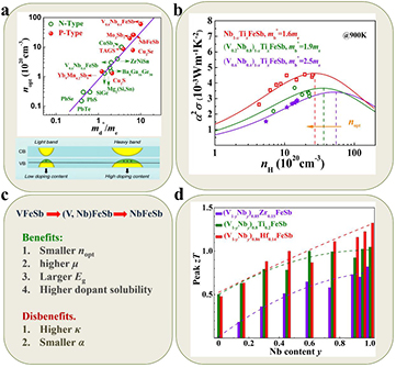
Figure 5. (a) The optimal carrier concentration nopt versus the density of state effective mass  for TE materials. The solid line is a guide for the eyes. Reproduced from [56]. CC BY 4.0. (b) Power factor of (V1−yNby)1−xTixFeSb samples as a function of hole concentration. The dashed lines indicate the optimal hole concentration for the samples with different Nb contents. [24] John Wiley & Sons. © 2015 WILEY-VCH Verlag GmbH & Co. KGaA, Weinheim. (c) The comprehensive influence of Nb substitution at the V site on peak zT. (d) Nb content dependence of peak zT of (V1−yNby)1−xXxFeSb (X = Ti, Zr, Hf) samples. Dashed lines show the trend of peak zT with Nb content. [87] John Wiley & Sons. © 2016 WILEY-VCH Verlag GmbH & Co. KGaA, Weinheim.
Download figure:
Standard image High-resolution imageWith the comparable carrier concentration (Ti content), the effective mass decreases and the power factor increases when y increases in (V1−yNby)1−xTixFeSb (figure 5(b)), and Nb0.8Ti0.2FeSb showed the highest power factor and lowest nopt [65]. This result indicates that the increased µ compensates for the decreased Seebeck coefficient, leading to a net enhancement of the power factor. The nopt of NbFeSb is smaller than that of VFeSb and can be reached within the solubility limit of Ti. Therefore, an easy-reaching nopt makes the optimal power factor easier to realize. Although Nb0.8Ti0.2FeSb has higher κL than (V0.6Nb0.4)0.8Ti0.2FeSb due to the dealloying of V, the difference in κL between them becomes smaller and smaller when the temperature increases (from 30% at room temperature to 15% at high temperature). It means that the increased κL will not degrade the high temperature zT too much, and that the enhanced power factor is more important. Further, an electronic band structure calculation reveals that NbFeSb has a larger band gap than VFeSb [87]. It is a preferable characteristic in thermoelectrics because the bipolar effect can be suppressed. Finally, a higher zT of 1.1 was achieved in Nb0.8Ti0.2FeSb at 1100 K [65]. Figure 5(c) shows the comprehensive influence of Nb substitution at the V site, and a similar phenomenon has also been found in Zr and Hf doped alloys. The peak zT of (V1−yNby)1−xXxFeSb (X = Ti, Zr, Hf) shows an increasing tendency when the Nb content increases (figure 5(d)) [87].
Heavy band (high effective mass) TE semiconductors call for high carrier concentrations to optimize their power factors. Routine doping is usually limited by two factors: the dopant solubility and doping efficiency. A high concentration of dopants may bring strong scattering to charge carriers and thus deteriorate the mobility. Hence, a dopant with a high doping efficiency will be preferable in tuning carrier concentration. Hf is a better dopant than Ti and Zr in the RFeSb system, although they belong to the same column in the periodic table [56]. As shown in figure 6(a), the carrier concentrations of the doped NbFeSb samples with different dopants are smaller than the theoretically predicted values, indicating that these dopants incompletely provide carriers. A similar phenomenon is also found for an Sn-doped ZrCoSb HH system [44]. But for an n-type ZrNiSn HH compound, the Sb dopant is highly efficient in providing electrons [90]. Comparatively speaking, Hf doping in NbFeSb is more efficient than Zr/Ti doping. At a carrier concentration of ~2 × 1021 cm−3, the corresponding room temperature carrier mobility for Hf-, Zr- and Ti-doped samples is 18.4, 15.0 and 13.8 cm2 V−1 s−1, indicating that a lower doping content for Hf-doped NbFeSb is beneficial for a relatively higher carrier mobility due to the reduced alloy scattering of carriers. Therefore, at the same carrier concentration, the Hf-doped NbFeSb has higher power factors than Zr- and Ti-doped samples (figure 6(b)). The doping efficacy of dopants should be carefully considered.
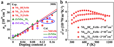
Figure 6. (a) Room carrier concentration versus doping content for NbFeSb ZrNiSn and ZrCoSb HH compounds. The lines were calculated assuming that each doping atom supplies exactly one carrier. (b) Power factor comparison for Hf, Zr, Ti doped NbFeSb samples under a similar carrier concentration of ~2 × 1021 cm−3 (blue ellipse in (a)). Reproduced from [56]. CC BY 4.0.
Download figure:
Standard image High-resolution imageAlthough HH alloys are viewed as high temperature TE materials, the enhancement of their room temperature performance is also significant for practical application. Recently, it was reported that Ti-doped NbFeSb could achieve a record high power factor of 106 µW cm−1 K−2 at ambient temperature by simply increasing the hot-pressing temperature [91]. Temperature-dependent electrical conductivity and Hall mobility indicates that the origin of such a high power factor should be ascribed to the variation in the carrier scattering mechanism, which noticeably improves the mobility. This work demonstrates that tuning the carrier scattering mechanism can be utilized as an effective approach to enhance mobility and hence the power factor [92].
4. Improving thermal transport
For solid-state materials, κ mainly consists of three parts, e.g. the electronic thermal conductivity κe, the lattice thermal conductivity κL, and the bipolar thermal conductivity κb. Using Wiedemann–Franz–Lorenz law, κe = LσT, the equation for zT can be re-written as:
Here L is the Lorenz number, which does not vary much from material to material, remaining in the range of 1.6–2.5 × 10⁻⁸ V2 K−2. In order to obtain a high zT, a high electronic thermal conductivity is not a problem, while a low lattice thermal conductivity κL and a low bipolar conductivity κb are desirable. For HH materials, typical NbFeSb-based alloys continuously decrease κ till 1200 K, and no significant bipolar effect is observed, indicating a negligible κb for NbFeSb-based TE materials. Therefore, a further reduction of thermal conductivity lies in suppressing κL. The main approach to obtain low κL is to enhance phonon scattering by introducing multiscale scattering centers.
The formation of solid solutions will induce strong alloying disorder (mass and strain field fluctuations) and lead to an enhanced point defect scattering of phonons as a result, significantly reducing κL [93, 94]. Since it was first proposed by Ioffe in the 1950s [95], forming solid solutions has long been regarded as a remarkably effective strategy to improve the zT of TE materials, even though it will cause some deterioration to the carrier mobility.
For RFeSb-based alloys, one should be careful when decreasing the thermal conductivity by forming a solid solution because of the concurrent influence on electrical transport. When (V, Nb)FeSb solid solutions are studied as n-type materials, the dopant Co at the Fe site is usually used to optimize the electron concentration, and Nb alloying at the V site has been proven to be useful in lowering the thermal conductivity due to the introduction of strong point defect scattering [53, 83]. Actually, due to alloy scattering, (V, Nb) alloying also deteriorates the electron mobility in n-type (V, Nb)FeSb solid solutions, but the decrease of κL plays a dominant role, and consequently the zT is enhanced. However, as has been mentioned previously, RFeSb-based alloys have better p-type performance due to the larger NV of the valence band [66]. Compared to ternary NbFeSb, although forming (V, Nb)FeSb solid solutions is indeed effective in suppressing κL, it is eventually proven to be harmful to carrier mobility, band gap and dopant solubility [65, 87]. Hence, zT can be enhanced in n-type alloys but degraded in p-type alloys by the formation of solid solutions. Fortunately, the optimal doping content in p-type alloys (e.g. 20% Ti or 14% Hf) is much higher than in n-type (e.g. 1.5% Co), which also leads to strong point defect scattering and a comparably low κL. As shown in figure 7(a), with an increase in Ti content, the κL difference between Nb1−xTixFeSb and (V1−yNby)1−xTixFeSb keeps decreasing, and figure 7(b) shows that, with optimal Ti or Hf content, the variation of V content has an unremarkable effect on the alloys' κL.

Figure 7. (a) Room temperature lattice thermal conductivity versus nominal Ti content x for (V1−yNby)1−xTixFeSb samples. [24] John Wiley & Sons. © 2015 WILEY-VCH Verlag GmbH & Co. KGaA, Weinheim. (b) V content dependence of room temperature κL for the undoped and Zr, Ti, Hf-doped Nb1−xVxFeSb samples. The dashed lines are a guide for the eye. [87] John Wiley & Sons. © 2015 WILEY-VCH Verlag GmbH & Co. KGaA, Weinheim.
Download figure:
Standard image High-resolution imageReplacing the Ti dopant by more efficient Hf is not only beneficial for enhancing the electrical properties, but also favorable for decreasing thermal conductivity because the heavier Hf doping will bring stronger mass fluctuation and cause stronger phonon scattering. Thus, a synergistic optimization in power factor and κL was observed for Hf-doped NbFeSb-based alloys, contributing to a high zT of ~1.5 at 1200 K [56]—much higher than Ti-doped ones.
Ta is also a group VB element, the same as V and Nb. What is the difference between Ta alloying and V alloying? Ta is often found together with Nb, occuring in the minerals tantalite, columbite and coltan (a mix of columbite and tantalite). These two elements have almost the same atom size, and are chemically similar in nature, much like Zr and Hf, which are also similar elements. Inspired by their similarity and the success of Hf alloying in ZrNiSn [40], Ta alloying in NbFeSb was performed to suppress lattice thermal conductivity while maintaining good electrical transport [35] due to the similar atomic size and chemical nature but a large mass fluctuation between Nb and Ta. It should be mentioned that Ta has a high melting point (3290 K) and hence the fabrication of single phase Nb1−xTaxFeSb solid solutions is challenging. This has been overcome by a levitation melting technique with strong electromagnetic stirring during the melting process (figure 8). Due to the remarkable reduction of thermal conductivity and the preservation of electrical properties, a record-high zT of ~1.6 at 1200 K for (Nb0.64Ta0.36)0.8Ti0.2FeSb and (Nb0.6Ta0.4)0.8Ti0.2FeSb can be obtained—~45% higher than that of Nb0.8Ti0.2FeSb [35].

Figure 8. (a) XRD patterns of (Nb1−xTax)0.8Ti0.2FeSb. (b) Fracture surface of (Nb0.6Ta0.4)0.8Ti0.2FeSb. (c) SEM and (d)–(h) EDX compositional mapping of the (Nb0.6Ta0.4)0.8Ti0.2FeSb sample. [35] John Wiley & Sons. © 2017 WILEY-VCH Verlag GmbH & Co. KGaA, Weinheim.
Download figure:
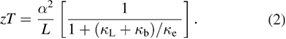
Standard image High-resolution imageThe strategies mentioned above mainly focus on scattering high frequency phonons by introducing point defects. Heat-carrying phonons cover a broad spectrum of frequency, and the κL is a sum of contributions of phonons with different frequencies. Thus, introducing hierarchical phonon scattering centers into the matrix, which could lead to a substantially reduced κL, has recently been proposed to improve TE performance [12, 96, 97]. However, the charge transport may also be significantly diminished by the introduced scattering centers, offsetting the beneficial contribution to zT. Therefore, maintaining high carrier mobility µ while greatly suppressing κL is key to improving the TE properties by introducing hierarchical scattering centers. To make this approach effective, the hierarchical scattering centers should scatter phonons more strongly than carriers [98]. Therefore, the zT of TE materials with an intrinsically high phonon mean free path lph and low carrier mean free path lc are more likely to be improved by using this approach. This can be most probably realized in heavy-band TE materials with a large band effective mass and low charge mobility.
P-type NbFeSb-based HH compounds are typical heavy-band TE materials with high κL but low carrier mobility. The Ioffe–Regel rule indicates that the electrical resistivity of alloys or intermetallic compounds normally saturates when the charge mean free path becomes comparable to the inter-atomic spacing and gives a minimum value to the carrier mobility [99]. The minimum electrical conductivity σmin and the minimum carrier mobility µmin can be roughly estimated by the formulas: σmin = 0.33e2p2/3a/ћ and µmin = σmin/(pe), where e, p, a and ћ are the unit charge, carrier concentration, lattice parameter, and the reduced Planck constant, respectively. Fu et al estimated the σmin and µmin of NbFeSb-based HH materials and found that the electrical conductivity and carrier mobility were very close to the Ioffe–Regel limits at high temperatures, indicating that more scattering centers would have a slight, even negligible, impact on high temperature electrical transport [77]. Therefore, hierarchical phonon scattering centers to scatter the phonons with different frequencies, including sub-microscale grain boundaries to target the low frequency phonons, atomic-scale point defects to scatter high-frequency phonons and enhanced electron–phonon interaction, are concurrently introduced to NbFeSb-based materials (figure 9(a)), leading to a substantially reduced κL. Figure 9(b) shows the calculated spectral lattice thermal conductivity for the Ti-doped and Fe excess NbFeSb compounds, demonstrating the efficacy of hierarchical phonon scattering centers in reducing κL. Coupled with the unchanged electrical properties, a significantly enhanced peak zT of 1.34 has been experimentally obtained at 1150 K for the grain-refined Nb0.75Ti0.25Fe1.05Sb, as presented in figure 9(c) [77].
Figure 9. (a) A schematic illustration showing hierarchical phonon scattering. The low frequency, high frequency and full frequency phonons are respectively scattered by sub-microscale grain boundaries (B), point defects (PD) and electrons (EP). (b) Phonon frequency dependence of spectral lattice thermal conductivity κs for the samples with different phonon scattering mechanisms. U represents the phonon–phonon Umklapp process and ωD is the Debye frequency. PDTi-doping and PDFe-excess donate point defect scattering due to Ti doping and Fe excess, respectively. (c) The temperature dependence of zT for a p-type NbFeSb system with intentionally designed hierarchical phonon scattering centers. Reproduced from [77]. CC BY 4.0.
Download figure:
Standard image High-resolution imageSimilar to p-type NbFeSb, introducing multiscale scattering centers is also efficient in p-type MCoSb (M = Ti, Zr, Hf). Forming solid solutions is the main strategy to increase point defect scattering, while nanostructuring and phase separation are two typical strategies to increase boundary scattering.
In MCoSb alloys, where M can be Ti, Zr, Hf or a combination of two or three, the high substitutability of the three lattice sites (M, Co, and Sb) provides ample opportunities to further depress the thermal conductivity. There have been some reports on reducing the thermal conductivity via elemental substitution at the three respective lattice sites, such as a combination of Ti and Zr (M site) [100], substitution of Co by Fe [45], Ir [101], or Rh [102], and Sb by Sn [103] or Ge [104]. Some theoretical calculations have also been conducted to investigate the effect of the mass difference and strain field fluctuation on the lattice thermal conductivity of MCoSb alloys [104, 105]. Culp et al investigated the influence of the substitution of Hf at the Zr site on TE properties. Point defect scattering remarkably reduces the thermal conductivity, which leads to a peak zT of 0.5 at 1000 K for ingot samples [43]. A similar result was reported by Kilian et al, whose samples were sintered with micron powders [106].
Although the thermal conductivity has been greatly reduced due to mass fluctuation in those (Zr, Hf)CoSb alloys, the lattice thermal conductivity is still very high. As mentioned above, point defects mainly scatter high frequency phonons, and boundary scattering can be introduced to further reduce the lattice thermal conductivity. To enhance boundary scattering, it is necessary to increase the boundaries by reducing grain sizes or introducing extra boundaries. For example, for p-type Hf0.5Zr0.5CoSb0.8Sn0.2, Yan et al have shown that the room temperature lattice thermal conductivity is only ~2.8 W m−1 K−1 when grain sizes are below 200 nm. With a comparable power factor, they achieved an improved zT of 0.8 at 973 K [59]. The key factors for achieving such small grain sizes are high energy ball milling and rapid sintering. We have also studied p-type nanostructured Zr1−xHfxCoSb0.8Sn0.2 solid solutions throughout the composition range. The results shown in figure 10 demonstrate that nanostructuring and isoelectronic substitution of Hf at the Zr site are feasible ways to reduce the lattice thermal conduction and enhance TE performance.
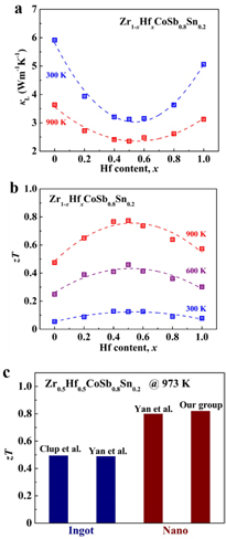
Figure 10. Hf content dependence of (a) κL, (b) zT for Zr1−xHfxCoSb samples. The dashed lines are a guide for the eye. (c) zT of ingot and nanostructured samples of Zr0.5Hf0.5CoSb0.8Sn0.2 by different groups. The data are from [43, 59].
Download figure:
Standard image High-resolution imageA combination of Hf and Ti is thought to be more effective in reducing the lattice thermal conductivity than that of Hf and Zr, considering the large differences in the atomic mass and size of Hf and Ti. This concept has been validated experimentally in n-type (Ti, Zr, Hf)NiSn systems [107]. Similarly, Yan et al achieved a peak zT of 1.0 with a low thermal conductivity of 2.7 W m−1 K−1 at 1073 K in Hf0.8Ti0.2CoSb0.8Sn0.2 due to stronger phonon scattering with larger differences in atomic mass and size [69] compared to that in Hf0.5Zr0.5CoSb0.8Sn0.2 [59].
HH nano-composites have also been investigated in the past to improve their TE properties. Generally, nano-inclusions in a HH matrix can be introduced by either mechanical mixing (ex situ) or nano-precipitation (in situ) processes. It is relatively straightforward and uncomplicated to obtain nano-composites with nano-inclusions by mechanical mixing, and the effects of nano-inclusions on the electrical and thermal transport properties of HH compounds have been systemically investigated [46]. For example, Poon et al investigated the relationship between the microstructure and TE properties of p-type Hf0.3Zr0.7CoSn0.3Sb0.7 with 20–300 nm ZrO2 nano-composites [108]. Due to the enhanced power factor and reduced lattice thermal conductivity, the Hf0.3Zr0.7CoSn0.3Sb0.7 nano-composites, with 1 vol.% of ZrO2 nano-inclusions, achieved a high zT of ~0.8 at 970 K, which increases by ~23% compared with that of the matrix ingot.
The in situ approach is the way in which nanoscale inclusions form within the homogeneous matrix via heterogeneous nucleation and growth, such as metastable phase decomposition and nanoscale precipitation. In the MCoSb system, when indium (In) was added into the mixed starting materials during induction melting, In can react with antimony which results in the formation of nanoscale InSb inclusions [109]. The phonon scattering is enhanced at the matrix/nano-inclusion interfaces, resulting in a reduction in lattice thermal conductivity.
Recently, it has been demonstrated that the concept of phase separation can also be applied to the p-type MCoSb system because intrinsic micrometer-scale phase separation can increase phonon scattering and reduce lattice thermal conductivity. Rausch et al reported that the partial substitution of Ti with Hf would result in phase separation in this system, which consisted of at least two stable Heusler phases (one rich in Ti and Sn, and the other rich in Hf and Sb). Subsequently, the thermal conductivity was reduced to 3.2 W m−1 K−1 in Ti0.5Hf0.5CoSb0.8Sn0.2, and a maximum zT of 0.9 was achieved at 973 K [110]. Furthermore, by fine tuning the Ti to Hf ratio for optimal phonon scattering in combination with optimal electronic properties by 15% Sn doping, Rausch et al achieved a maximum zT of 1.2 at 983 K for Ti0.25Hf0.75CoSb0.85Sn0.15 [55], comparable to the state-of-the art n-type Ti0.5Zr0.25Hf0.25NiSn0.998Sb0.002 (zT = 1.2 at 833 K) [42].
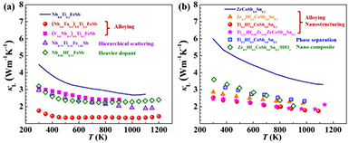
Since a high κL is a common problem for most reported HH materials, here we demonstrate the κL of RFeSb and MCoSb obtained by different strategies in figure 11, serving as a brief summary of this section.
Figure 11. The κL of (a) RFeSb- [35, 56, 65, 66, 77] and (b) MCoSb- [58, 59, 69, 78, 110] based compounds obtained by different strategies.
Download figure:
Standard image High-resolution image
5. Outlook
HH compounds contain hundreds of semiconductors with adjustable band gaps, which provide the possibility of abundant selections to engineer the band structure and enhance the TE properties. The strategies mentioned in this review could be a guide for future material design. For example, due to the high thermal conductivity but low carrier mobility of p-type NbFeSb-based compounds, forming nano-composites in this system may be useful to scattering phonons, while only slightly deteriorating carrier transport. The (Nb, Ta)CoSn HH system has a similar characteristic of an electronic structure with NbFeSb. The valence band of (Nb, Ta)CoSn has a higher degeneracy than the conduction band due to its specific pocket alignment. High-throughput transport and defect calculations have predicted their potential as high-performance p-type TE materials [111], but, to the best of our knowledge, only experimental results of n-type properties have been reported [50, 74, 112].
Besides the application in thermoelectrics, the specific structure and element constitution of HH materials allow for other multi-faced and tunable physical properties. Some ternary HH compounds already boast an impressive list of properties, such as magnetism [113], superconductivity [114] and heavy-Fermion behavior [115]. Together with the predicted topological properties using first-principles calculations, these materials provide an exciting opportunity for novel quantum phenomena [116–118], and the versatility of HH compounds ultimately paves the way towards multifunctional topological devices for spintronics and fault-tolerant quantum computing [80].
Inspired by the multi-faceted physical properties of HH materials, broadening the research domains is encouraged. More importantly, some similar material systems, such as full-Heusler (FH) compounds [119–123], Nowotny–Juza phases [8, 9, 124] as well as non-18 electron HH compounds [52, 125, 126], have recently shown increasing potential in thermoelectrics. Studies for these series of compounds are also highly encouraged.
The family of FH compounds, including metallic and semiconducting materials, shows unusual transport properties. For instance, the Co2TiZ (Z = Al, Si, Ge, Sn) system exhibits high Seebeck coefficients in a metallic system [119], and the high strength and low-cost semiconductor Fe2VAl has also been studied [120–123]. Therefore, we believe that there will be much potential application of FH materials in thermoelectrics. MgAgSb, a typical member of Nowotny–Juza phases, has a similar structure with HH compounds at high temperatures [80]. Its low temperature α phase (RT ~ 560 K) [127] has recently been discovered to be a promising p-type TE material with a peak zT of 1.1–1.4 near room temperature [8, 9]. Different from normal HH materials, α-MgAgSb shows intrinsically low κL due to its hierarchical weak chemical bonding. There must be more interesting phenomenon in other Nowotny–Juza compounds [124].
Due to the huge influence of the valence electron count on the electronic structure and physical properties of HH compounds, typical high performance HH TE compounds all exhibit 18 valence electrons and the 18-electron rule is a widely used criterion in the exploration of a possible TE phase in the HH family. However, some non-18 electron compounds have recently been reported to show good TE performance [52]. For example, the 19-electron NbCoSb compound is actually a composite of non-stoichiometric 18-electron Nb0.8CoSb compounds and metallic second phases. A pure phase and remarkable enhancement of TE performance can be achieved in 18-electron Nb0.8CoSb, which opens a new avenue to search for potential HH TE materials [125, 126].
In summary, the past few years have witnessed the rapid progress of HH materials on TE performance. In particular, the remarkable zT enhancement of RFeSb-based materials makes the p-type counterpart comparable with n-type MNiSn-based materials, and the significant advantages, such as low cost raw materials, long term thermal stability as well as excellent mechanical robustness, also facilitate large-scale device applications of HH materials. More work is needed for device assembly.
Acknowledgments
This work was supported by the National Science Fund for Distinguished Young Scholars (51725102) and the Natural Science Foundation of China (11574267, 51571177 and 51761135127).