
Abstract
Titanium dioxide (TiO2) is a widely used electron transport material in organic-inorganic hybrid perovskite solar cells (PSCs). In order to reveal the influence of an additional mesoporous TiO2 (mp-TiO2) layer on fabricating large-area perovskite solar cells using TiO2 as the electron transport layer, we have conducted a comprehensive study on the solution-processed PSCs with or without an additional mp-TiO2 layer. Photoemission spectroscopy measurement indicates that, compared with the compact TiO2 (cp-TiO2) layers, the mp-TiO2 layers possess a slightly larger work function, which will improve the electron extraction efficiency at the perovskite-TiO2 interface. The PSCs with an additional mp-TiO2 layer exhibit better performances than those with only a cp-TiO2 layer. They suffer from a smaller efficiency loss when enlarging the device area from 0.16 to 1.44 cm2 and exhibit a better long-term stability. About 89% of the initial efficiency is retained after keeping in dry air for 1000 h for the device with an active area of 1.44 cm2. For both cases, increasing the active device area is beneficial to long term stability, photoluminescence measurement indicates that this is result from the degradation of perovskite films starts at the margin of the cells. Our work implies the indispensable role of the additional mp-TiO2 layer for optimizing the performances of large-area PSCs using TiO2 as the electron transport layer.
Export citation and abstract BibTeX RIS

Original content from this work may be used under the terms of the Creative Commons Attribution 3.0 licence. Any further distribution of this work must maintain attribution to the author(s) and the title of the work, journal citation and DOI.
Introduction
Organic-inorganic perovskite solar cells (PSCs) have attracted intensive attention owing to its remarkable photoelectric performance [1–5]. In the recent years, the power conversion efficiency (PCE) of PSCs have rapidly climbed from 3.8% to 22.7% [6–16]. Much effort has been focused on improving the crystallographic quality [12, 17] and adjusting the composition of the perovskite layer [18–20] to improve the PCE and stability. As an essential part, the electron transport layer (ETL) also plays a crucial role in device performance. A number of ETL materials with different work function [13, 21] and conductivity have been used, resulting in different interfacial barrier [14] and interfacial resistance [22], and therefore affect the electron extraction efficiency at the interface between the perovskite and electron transport layers. Meanwhile, the electron transport layer play an important role on the morphology and crystallization of the top perovskite layer [23]. Among the ETL materials adopted for PSCs, titanium dioxide (TiO2) is one of the most widely used materials due to the excellent optoelectronic property, stability, and concise deposition processes [9]. The electronic properties of TiO2 are able to be adjusted with incorporation of Y [13], Al [24], Li [25] or In [22] cations. Interfacial recombination is further suppressed by contact passivation at the perovskite-TiO2 interface [14, 15].
Depending on the fabrication techniques, the TiO2 layers exhibits different structural, mechanical, optical and electrical properties [26–28]. A compact layer (cp-TiO2) with dense and uniform surface is formed by pyrolysis of a thin film of organic titanium compounds [29], while a mesoporous layer containing nanoparticles with high specific surface area is prepared by sintering TiO2 nanoparticle precursors [9]. Here, to reveal the influence of an additional mesoporous TiO2 (mp-TiO2) layer on fabricating large-area perovskite solar cells, we have conducted a comprehensive study on the PSCs with or without an additional mp-TiO2 layer. we used a straightforward solution-processed method to fabricate PSCs with two different structures, namely, fluorine-doped tin oxide (FTO)/cp-TiO2/perovskite/2,2',7,7'-Tetrakis-(N,N-di-4-methoxyphenylamino)-9,9'-spirobifluorene (Spiro-OMeTAD)/Au and FTO/cp-TiO2/mp-TiO2/perovskite/Spiro-OMeTAD/Au. A cp-TiO2 layer or a sequentially fabricated cp-TiO2/mp-TiO2 layer is used as the ETL in PSCs with small (0.16 cm2) or large active area (1.44 cm2). The PSCs with a cp-TiO2 layer and a cp-TiO2/mp-TiO2 layer show champion power conversion efficiencies (PCE) of 12.94% and 15.12% in 0.16 cm2 devices, 11.85% and 14.76% in 1.44 cm2 devices, respectively. The relatively higher PCE for the PSCs with an additional mp-TiO2 layer is attributed to the increase of the short circuit current. The slightly larger work function of the additional mp-TiO2 layer as measured by photoemission spectroscopy improves the electron extraction efficiency at the perovskite-TiO2 interface. Furthermore, the long term stability of the devices has been investigated. It was found that the PSCs with an additional mp-TiO2 layer exhibit a better long-term stability. For both cases, increasing the active device area is beneficial for the stability. The PSCs with an additional mp-TiO2 layer with an active area of 1.44 cm2 retain 89% of the initial efficiency after keeping in dry air for 1000 h.
Experiment section
Materials and reagents
Unless otherwise stated, all materials were purchased from Sigma-Aldrich or Aladdin. FTO-coated glass was purchased from Pilkingdon and the mesoporous TiO2 (18NR-T) paste was purchased from Dyesol. All materials were used without further purification.
Solar cell fabrication
Photovoltaic devices were fabricated on FTO-coated glass. The etched FTO glass substrates were sequentially cleaned by ultrasonication in detergent, deionized water, acetone, and isopropanol for 20 min. After being dried with high-purity nitrogen gas, they were then treated with UV-ozone for 20 min before film deposition. The cp-TiO2 layer was prepared on the FTO substrate by spin coating of titanium diisopropoxide bis (acetylacetonate) solution (75% in isopropanol, Sigma) diluted in 1-butanol (1:10 weight ratio) at 2000 rpm for 30 s, and then the substrates were annealed on a 135 °C platform for 10 min. After cooling down to room temperature, we repeated the above process again and subsequent annealing it at 500 °C for 30 min. The mp-TiO2 layer was prepared on the cp-TiO2 layer by spin coating the 18NR-T paste diluted with anhydrous ethanol (1:7 weight ratio) at 3000 rpm for 30 s and then annealed at 500 °C for 30 min. All the above operations were carried out in the atmosphere. After the preparation of TiO2 layer, the substrates were put into a glove box with nitrogen atmosphere. The methylammonium lead iodide (MAPbI3) solution was prepared by dissolving 1 mmol methylamine iodine (MAI) and 1 mmol PbI2 in 1 ml anhydrous dimethyl sulphoxide (DMSO):N,N-dimethylformamide (DMF) (3:7, volume ratio), and then the precursor solutions were filtered by a 0.22 μm PTEF filter before spin coating. The perovskite solution was deposited on the cp-TiO2 or cp-TiO2/mp-TiO2 layer by spin coating at 5000 rpm for 30 s. During spin coating, chlorobenzene was dripped on the rotating film 6 ∼ 8 s after the start of the program, and then perovskite film was annealed at 100 °C for 10 min. The Spiro-OMeTAD solution was prepared by dissolving 75 mg spiro-OMeTAD, 28 ul 4-tert-butylpyridine and 18 ul bis sulfonimide lithium salt (520 mg ml−1 in acetonitrile) in chlorobenzene (1 ml). The Spiro-OMeTAD solution was spin coated at a rate of 3000 rpm for 25 s. Finally, an Au electrode with thickness of 100 nm was deposited by thermal evaporation with a shadow mask to define the active area.
Measurements and characterization
The J-V characteristics were tested in the ambient atmosphere under 1 sun conditions (AM1.5 G) with a solar simulator system (ABET Technologies Sun 3000) without aperture mask. The light intensity was calibrated using a NREL-calibrated KG5 filtered silicon reference cell. The voltage scan rate was 50 mV s−1 in the reverse direction (from 1.2 to −0.2 V). No device preconditioning was applied before the measurement for all devices. The surface morphology of TiO2 and perovskite films and the cross sectional structure of the whole PSCs were characterized by scanning electron microscopy (SEM) (ZEISS Merlin). X-ray photoelectron spectroscopy (XPS) and ultraviolet photoelectron spectroscopy (UPS) measurements were carried out using ThermoFisher Escalab 250Xi spectrometer. The monochromatic x-ray source for XPS was Al Kα (1487.6 eV), and during the experiment, the vacuum of the analysis chamber was kept around 1 × 10⁻⁹ mbar. The Ultraviolet light for UPS was He Ι (21.2 eV). During the measurements, a bias of −5 V was applied to the sample, and the vacuum of the analysis chamber was about 3 × 10⁻⁸ mbar. X-ray diffraction (XRD) was used to investigate the structure of the perovskite films and implemented by Bruker D8-Advance with Cu Kα radiation (λ = 1.5406 Å). The transmission spectrum of the sample was investigated by ultraviolet-visible spectrophotometer (Shimadzu UV-2600). Photoluminescence was measured using a HORIBA Scientific system, the sample were excited by a continuous laser with a wavelength of 633 nm.
Results and discussion
XPS measurements were carried out to analyze the chemical composition of the cp-TiO2 and mp-TiO2 layers. Figures 1(a) and (b) compare the XPS spectra of Ti 2p and O 1 s of the cp-TiO2 and cp-TiO2/mp-TiO2 films, respectively. The Ti 2p1 and Ti 2p3 peaks are located at the binding energies of 464.4 and 458.7 eV, which is consistent with the result reported elsewhere [22, 30]. The O1s signals consist of a major peak located at 530.1 eV and a minor peak at 531.2 eV. The former corresponds to the oxygen bound with Ti, while the latter is ascribed to the hydrated oxygen [30, 31]. The overall Ti : O ratio is 1:2.33 for cp-TiO2 and 1:2.15 for mp-TiO2, respectively. The proportion of oxygen is about 70.0% (68.3%), of which hydrate oxygen accounts for about 13.6% (10.4%) in the cp-TiO2 (mp-TiO2) films. The work function (WF) of ETL plays an important role in exciton separation and charge transport in devices. We conducted UPS measurement to obtain the WF and valence band structure of cp-TiO2 and mp-TiO2. According to the photoemission cutoff shown in figure 1(c), we obtain a WF of 4.31 eV (WF = hν − cutoff) for cp-TiO2 and 4.37 eV for mp-TiO2, respectively. The slight increase of WF for mp-TiO2 compared with cp-TiO2 originates from the lower proportion of excessive hydrated oxygen [32]. As shown in figure 1(d), the valence band maximum of cp-TiO2 and cp-TiO2/mp-TiO2 were 3.54 eV and 3.59 eV below the Fermi level, respectively.

Figure 1. The XPS and UPS spectra of FTO/cp-TiO2 and FTO/cp-TiO2/mp-TiO2. (a) XPS spectra of Ti 2p peak. (b) XPS spectra of O 1 s peak. (c) Work function of FTO/cp-TiO2 and FTO/cp-TiO2/mp-TiO2. (d) Valence band structure of FTO/cp-TiO2 and FTO/cp-TiO2/mp-TiO2.
Download figure:
Standard image High-resolution imageFigure 2(a) shows the transmittance spectra of FTO, FTO/cp-TiO2 and FTO/cp-TiO2/mp-TiO2. Within the visible light region from 400 nm to 800 nm, the FTO sample exhibits the largest transmittance (roughly 80%), while the FTO/cp-TiO2 sample shows a transmittance 5%–8% lower than FTO. Compared with the FTO/cp-TiO2 layer, the transmittance of the FTO/cp-TiO2/mp-TiO2 sample exhibits a slight decrease (3%–5%) due to the porous morphology and the increased thickness, as shown in the SEM cross-sectional images of the complete devices (figure 2). In the cells with a cp-TiO2/mp-TiO2 layer, the average thicknesses of TiO2 layer and perovskite layer are 166 nm and 218 nm, respectively, while the values are 109 nm and 215 nm in PSCs with only a cp-TiO2 layer. Although the thicknesses of TiO2 layers are different, the thicknesses of perovkite layers are almost the same in the two PSCs.

Figure 2. (a) Transmittance spectra of bare FTO, FTO/cp-TiO2, and FTO/cp-TiO2/mp-TiO2. (b) Cross-sectional SEM images of the solar cells with structure of FTO/cp-TiO2/perovskite/Spiro-OMeTAD/Au and FTO/cp-TiO2/mp-TiO2/perovskite/Spiro-OMeTAD/Au.
Download figure:
Standard image High-resolution imageFigures 3(a) and (b) show the top-view SEM images of cp-TiO2 deposited on FTO and mp-TiO2 deposited on FTO/cp-TiO2, respectively, presenting different morphologies. The surface of cp-TiO2 is smoother than the cp-TiO2/mp-TiO2 layer. The latter consists of nanoparticles with a size in the range of 10–50 nm resulting in mesoporous structure. Figures 3(c) and (d) display the morphology of perovskite films grown on cp-TiO2 and cp-TiO2/mp-TiO2 layer. Both capping layer exhibit good homogeneity with the grain size in the range of 100–300 nm. From the cross-sectional SEM image, there is no obvious difference about the grain size of perovskite that formed on top of cp-TiO2 and mp-TiO2.
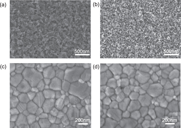
Figure 3. Top-view SEM images of (a) cp-TiO2 grown on FTO and (b) mp-TiO2 grown on cp-TiO2 (c) MAPbI3 grown on cp-TiO2 and (d) MAPbI3 grown on cp-TiO2/mp-TiO2.
Download figure:
Standard image High-resolution imageIn figures 4(a) and (c), the current density-voltage (J-V) characteristics of the champion PSCs with cp-TiO2 and cp-TiO2/mp-TiO2 as the ETL is presented. Devices with different active area are compared. The active area is determined by the overlap of bottom FTO pattern and the uppermost gold electrode. The smaller and larger devices have an active area of 0.16 and 1.44 cm2, respectively, as shown in the photographs in figures 4(b) and (d). Compared with the devices with only a cp-TiO2 layer, the devices with an additional mp-TiO2 layer exhibit a larger short-circuit current density (Jsc). The larger Jsc is ascribed to the increased WF by the additional mp-TiO2 layer, which will improve the electron extraction efficiency at the perovskite-TiO2 interface. Results of previous research indicate that appropriate increase of interfacial energy offset is helpful for inducing highly efficient carrier transfer [33]. Meanwhile, the devices with an additional mp-TiO2 layer possess higher open circuit voltage (Voc) and filling factor (FF), resulting in a significant increase in PCE. We believe the additional mp-TiO2 layer will eliminate the direct contact between the perovskite layer and the FTO electrode [34] and therefore dramatically reduce the leaking current from the perovskite layer to the FTO electrode. Although the additional mp-TiO2 layer would slight increase the series resistance of the devices, but considering its benefits, mp-TiO2 layer is still advantageous. The highest efficiency we have obtained is 15.12% for the small-area devices with an additional mp-TiO2 layer. The Voc (1059 mV) and FF (>70%) are comparable with the best-performed devices with similar structure as reported in the literature [22], while the relatively smaller Jsc is ascribed to the thinner perovskite layer (about 200 nm) and incomplete light absorption in our experiment [35].
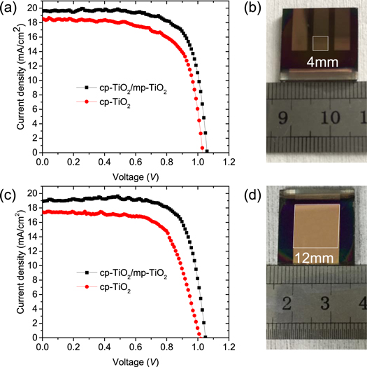
Figure 4. J-V curves of the champion devices and photographs of devices with difference active area. (a) and (b) The smaller devices with an active area of 0.16 cm2. (c) and (d) the larger devices with an active area of 1.44 cm2.
Download figure:
Standard image High-resolution imageWe have further investigated the influence of an additional mp-TiO2 layer when increasing the device area from 0.16 to 1.44 cm2. Photovoltaic parameters of the champion devices are summarized in table 1. For both cases with or without an additional mp-TiO2 layer, increasing device area results in a slight decrease of PCE. It is still a challenge to obtain high-uniformity film on large area devices. Under the same experiment condition, it is easier to obtain high-quality films in small area devices. And the larger series resistance of FTO electrodes in larger area devices leads to the decrease in PCEs [36]. However, the devices with an additional mp-TiO2 layer suffer from a smaller efficiency loss. The best PCE of the larger devices with cp-TiO2/mp-TiO2 as the ETL is 97.6% of the smaller ones, while the case for cp-TiO2 is 91.6%. Out results indicate that the additional mp-TiO2 layer is beneficial to large area devices. An additional mp-TiO2 layer may fill the nanosized voids of the underlying cp-TiO2 layer and further reduces the direct contact between perovskite and FTO. Such effect is more obvious in larger devices because for larger area devices it is possible of containing more nanosized voids. As a result, the performance of the larger devices with only a cp-TiO2 layer decline more seriously in comparison to the devices with an additional mp-TiO2 layer. In fact, the uniformity of the ETL layer plays an important role on the device reproducibility [37, 38]. Statistical distribution of Jsc, Voc, FF and PCE of our devices with different active area and device structure are displayed in figure 5. The parameters fluctuate in a relatively small range, indicating a rather good reproducibility of devices. The reproducibility is notably improved by the additional mp-TiO2 layer.
Table 1. Photovoltaic parameters for the champion cells with or without an additional mp-TiO2 layer.
| ETL/active area | Jsc (mA cm−2) | Voc(mV) | FF(%) | PCE(%) | |
|---|---|---|---|---|---|
| cp-TiO2/mp-TiO2 | 0.16 cm2 | 19.62 | 1059 | 72.75 | 15.12 |
| cp-TiO2/mp-TiO2 | 1.44 cm2 | 19.00 | 1049 | 74.03 | 14.76 |
| cp-TiO2 | 0.16 cm2 | 18.50 | 1032 | 67.74 | 12.94 |
| cp-TiO2 | 1.44 cm2 | 17.51 | 1018 | 66.43 | 11.85 |

Figure 5. Statistic distribution of the photovoltaic parameters for cells with different active area and device structures. (a) Jsc. (b) Voc. (c) FF. (d) PCE.
Download figure:
Standard image High-resolution imageIn order to investigate the long-term stability, the devices were stored in dark and dry air (humidity < 30%) and measured every two days under AM1.5 G at ambient environment. Figures 6(a) and (b) show the normalized PCE as a function of testing time in a period >40 days. The smaller (larger) device with cp-TiO2/mp-TiO2 maintains 80.6% (89.0%) of the initial PCE after 1000 h, whereas that with a cp-TiO2 layer retained only 73.7% (75.0%) of the initial PCE. Our result indicates that the devices with a cp-TiO2 ETL undergo a greater degree of degradation, while the devices with an additional mp-TiO2 layer show enhanced stability. Furthermore, for both cases, increasing the device area is beneficial to long term stability.

Figure 6. (a) Stability test of PSCs on smaller area devices. (b) Stability test on larger active area device. (c) Photoluminescence spectra acquired from the spots near the device edge of the cp-TiO2 and (d) cp-TiO2/mp-TiO2 cells. (e) Photoluminescence intensity as a function of the distance to the gold electrode edge. (f) Schematic diagram of device degradation.
Download figure:
Standard image High-resolution image
Photoluminescence (PL) has been used as a measure for characterizing the degradation of our solar cells after keeping in air for more than 40 days. PL signals with a central wavelength at 769 nm [39] were acquired from different spots near the edge of the top gold electrode, as shown in figures 6(c) and (d). The PL intensity as a function of location with respect to the gold electrode edge is plotted in figure 6(e). No PL signal was observed from the exposed perovskite region on which no gold layer is covered, indicating a complete degradation. The region covered with the gold layer show a variable PL intensity depending on the distance to the edge of the gold electrode. Weaker PL was observed from the spots closer to the edge, while a saturated PL intensity was observed about 250–300 μm away from the edge. Compared with the device with only a cp-TiO2 layer, the device with an additional mp-TiO2 layer exhibits a relatively stronger PL intensity near the edge. The result suggests that the additional mp-TiO2 is helpful for protecting the perovskite layer from degradation, this may be attributed to less hydrates on the mp-TiO2 and its mesoporous structure could reduce the infiltration of air. We propose that the PL intensity variation is caused by degradation of the perovskite film near the device margin, as illustrated in figure 6(f). Water and oxygen molecules at ambient environment infiltrate into the cell from the device edge, and then react with perovskite to form PbI2 [40] or intermediate products, such as MA4 PbI6·2H2O [41]. The result of the degradation is the escape of MAI from MAPbI3. On the other hand, the central part of the perovskite film is protected to some extent by the compact metal electrode. Because small-area devices have relatively larger proportion of boundary area than large-area devices, increasing the active device area is beneficial to long term stability.
Conclusion
In summary, we have fabricated PSCs using cp-TiO2 and cp-TiO2/mp-TiO2 as ETL with smaller (0.16 cm2) and larger (1.44 cm2) device area and investigated the influence of the additional mp-TiO2 layer on photovoltaic performance. The mp-TiO2 layer possesses a slightly larger work function, which was in favor of the electron extraction at the perovskite-TiO2 interface. The improvement of PCE by using cp-TiO2/mp-TiO2 as ETL is mainly attributed to the increase in Jsc. The performance differences are more pronounced for large area PSCs with or without an additional mp-TiO2 layer. We have also investigated the stability and found the cp-TiO2/mp-TiO2 based PSCs perform better than the cp-TiO2 based devices in stability. For both cases, increasing the active device area is beneficial to long term stability, because the initial degradation of perovskite film takes place near the edge of the device. Our work implies that the additional mp-TiO2 layer is of importance for optimizing the device performances on both small and large PSCs.
Acknowledgments
The work was financially supported by National Natural Science Foundation of China (11574403 and 11374374) and Guangzhou Science and Technology Project (201607020023).
Conflict of interest
The authors declare no competing financial interest.