Abstract
The effect of electron injection on minority carrier transport in Si-doped β-Ga2O3 Schottky rectifiers with 18 MeV alpha particle exposure (fluences of 1012–1013 cm−2) was studied from room temperature to 120°C. Electron Beam-Induced Current technique in-situ in Scanning Electron Microscope was used to find the diffusion length of holes as a function of duration of electron injection and temperature for alpha-particle irradiated rectifiers and compared with non-irradiated reference devices. The activation energy for electron injection-induced effect on diffusion length for the alpha-particle irradiated sample was determined to be ∼ 49 meV as compared to ∼74 meV for the reference sample. The decrease in activation energy of the electron injection effect on diffusion length for irradiated sample is attributed to radiation-induced generation of additional shallow recombination centers closer to the conduction band edge.
Export citation and abstract BibTeX RIS

This is an open access article distributed under the terms of the Creative Commons Attribution Non-Commercial No Derivatives 4.0 License (CC BY-NC-ND, http://creativecommons.org/licenses/by-nc-nd/4.0/), which permits non-commercial reuse, distribution, and reproduction in any medium, provided the original work is not changed in any way and is properly cited. For permission for commercial reuse, please email: oa@electrochem.org.
Gallium Oxide is an emerging transparent conductive oxide with an ultra-wide bandgap of ∼4.8eV.1–9 Its high bandgap, together with an electric breakdown field of 8 MV/cm and high electron saturation velocity of 2 × 107 cm/s, makes it an attractive candidate for high power applications and solar blind detectors. The β-polymorph of Ga2O3 is the most stable out of all its forms and is readily available in high crystalline quality large area wafers and thick epitaxially grown films.2,5,7,9 The research and development of β-Ga2O3 bipolar technology is still in its early phase. So far, devices utilizing n-type conductivity have been fabricated: field effect transistors, Schottky rectifiers, sensitive solar-blind photodetectors.2,10–13 Additionally, the existence of p-type conductivity at high temperatures due to ionized vacancies has been shown.14 Moreover, β-Ga2O3 has high bond strength and vacancy formation energy,2 making it robust in radiation-harsh environments.15
In recent times, there's a surge of interest in characterization of radiation hardness of n-type β-Ga2O3 devices with conditions matching those in the space applications. Reports on the material properties and defects incurred due to neutron, electron, proton and gamma-ray radiation sources are surfacing,15–22 with the latest study being on alpha particle exposure.23 In general, for the tests performed so far, electron mobility degrades due to introduction of trap levels from radiation damage. In case of alpha-particle irradiated β-Ga2O3 Schottky rectifiers, electron removal rates of ∼406–728 cm−1 have been reported.23 Such degradation reduces the diffusion length of minority carriers, similar to the previous reports for gamma-irradiated GaN High Electron Mobility Transistors and high-energy electron irradiated β-Ga2O3 Schottky structures.18,24–26
Electron injection has proven to be a robust technique to enhance the minority carrier diffusion length in GaN and ZnO devices.27–30 Recently, this study was also extended to β-Ga2O3.31 In this article, we demonstrate the impact of electron injection on minority carrier diffusion length in alpha-particle irradiated β-Ga2O3.
Experimental
The samples involved in the study were fabricated on β-Ga2O3 single crystal substrates with 650 μm thickness and [001] orientation fabricated with edge-defined film-fed growth method (Tamura Corporation, Japan). Hall measurements after Sn doping showed a carrier concentration of 2.2 × 1018 cm−3 on this n+-substrate.16 A 20 μm-thick epitaxial Si-doped n-type Ga2O3 (∼8.3 × 1015 cm−3) was grown by Halide Vapor Phase Epitaxy (HVPE). After growth, the epitaxial layer was subjected to electromechanical polishing for planarization, subsequently reaching a thickness of ∼7 μm.
Vertical homoepitaxial Schottky rectifiers were fabricated by forming ohmic contacts using blanket electron-beam deposition of Ti/Au (20 nm/80 nm) on the back side of the stack. Top Schottky contacts (Ni-20 nm/Au-80 nm) were fabricated in a circular shape with varying diameters by standard lithography, metal deposition and lift-off technique. The measurements were performed on a contact with 210 μm diameter. A schematic diagram of the cross-section of the structure is shown in Fig. 1. Some rectifiers were exposed to 18 MeV alpha particle beam (fluences of 1012–1013 cm−2) using MC-50 Cyclotron at the Korea Atomic Energy Research Institute. The penetration range of the alpha particle beam in the sample was 80 μm. More details about the fabrication and irradiation process can be found in the study by Yang et al.23 A set of control devices (hereon called "reference") was used for comparison.
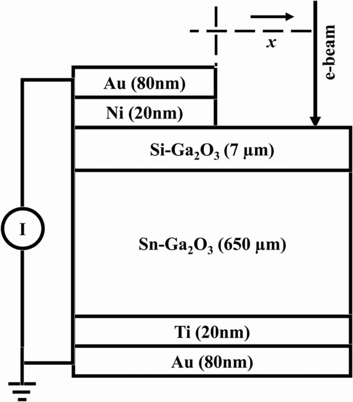
Figure 1. A schematic diagram of the structure and the measurement configuration used in the experiments.
The effect of electron injection on minority carrier transport in alpha-irradiated and reference Si-doped β-Ga2O3 Schottky rectifiers was studied using Electron Beam-Induced Current (EBIC) in-situ in Philips XL30 Scanning Electron Microscope (SEM) with integrated Gatan heater and controller in the temperature range from 23°C to 120°C. Planar configuration of EBIC line-scan technique32–35 was employed to measure the diffusion length (L) of minority carriers (holes, in this case). The SEM beam of 10 keV energy was used in the electron injection experiments, which resulted in an absorbed current of 0.4 nA and electron range of 0.4 μm in the material.36 The line-scans were performed by scanning the electron beam from the edge of the Schottky contact outwards, such that the direction of movement is perpendicular to the edge of the contact. A schematic diagram of the measurement configuration is shown in Fig. 1. During the line-scans, which lasted 6 seconds each, the current, induced due to the electron beam, was first amplified by Stanford Research Systems Low-Noise Amplifier (SR570) and then measured with Keithley DMM 2000 digital multimeter interfaced with a home-built software for data recording. The effect of electron injection was induced in the structures by repetitive scanning (400 s) at the same location in the vicinity of the Schottky contact.
Because the samples are very sensitive to electron beam irradiation, a new location was chosen for measurements at each temperature to remove any possibility of uncontrolled electron injection. The diffusion length was extracted from a single line-scan for each temperature at a new location to find the zero-injection diffusion length and calculate the activation energy for temperature-dependent diffusion length change. Each EBIC line-scan took 6 s to complete, which has virtually no impact on L. The same study is then repeated at each temperature with continuous non-stop line-scans of 6 s, for a total injection time of 400 s, inducing the changes of L. During electron injection, the current induced by the electron beam was continuously recorded.
Results and Discussion
Fig. 2 inset (upper-left) shows the time evolution of EBIC signal as a function of distance from the junction. The diffusion length for the minority carriers is calculated by fitting EBIC line-scan data to Equation 1 of empirical origin,32–35
![Equation ([1])](https://content.cld.iop.org/journals/2162-8777/8/7/Q3050/revision1/d0001.gif)
In this equation, I is the recorded current; I0 is a scaling constant; x is the distance of the electron beam from the junction; L is the diffusion length and α is the surface recombination velocity taking values from -3/2 to -1/2. Moreover, the fit is performed in the vicinity of the "knee" of the EBIC line-scan decay, such that x>2L34,37 to ensure the accuracy of L. The fit is further simplified by linearizing Equation 1, as shown in Fig. 2 (bottom-right inset). Furthermore, α = -3/2 is used throughout the analysis as it results in the best fit of the EBIC line-scan data.
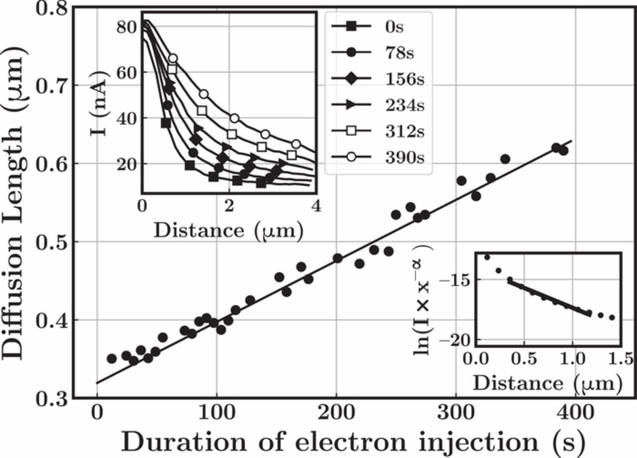
Figure 2. Hole diffusion length dependence on the duration of electron injection at 120°C. Inset (Top-left): EBIC line scans plotted at various durations of electron injection process. (Bottom-right): Arrhenius plot for linear fit according to the Equation 1.
This analysis is applied to the electron injection study by calculating L for every collected EBIC line-scan. Fig. 2 shows the linear increase of L with electron injection duration in alpha-irradiated β-Ga2O3 at 120°C. The electron injection-induced increase of L additionally manifests itself in the upper-left inset of Fig. 2, where every subsequent line-scan shows a slower decay of the EBIC amplitude due to an increase in L. The same trends are as well preserved in the reference sample, but the values of L, corresponding to zero-electron injection at each temperature, as well as the rate of L increase with duration of electron injection are significantly larger.31
While minority hole diffusion length exhibits a pronounced increase with duration of electron injection (cf. Fig. 2) at all temperatures used in this research, L dependence on temperature at zero-dose electron injection shows the opposite trend, namely it decreases with increasing temperature. For reference structure, L decreases from 427 nm to 332 nm between 23°C and 120°C. Alpha-irradiated structure shows L decrease from 378 nm to 324 nm for the same temperature range. This is shown in Figs. 3, 4.
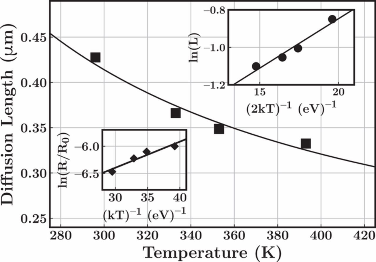
Figure 3. Temperature dependence of diffusion length for the reference structure. Inset (top-right): Arrhenius plot for Equation 2, used in the calculation of activation energy for diffusion length change with temperature. Inset (bottom): Arrhenius plot for Equation 3, used in the calculation of activation energy for diffusion length change due to electron injection.
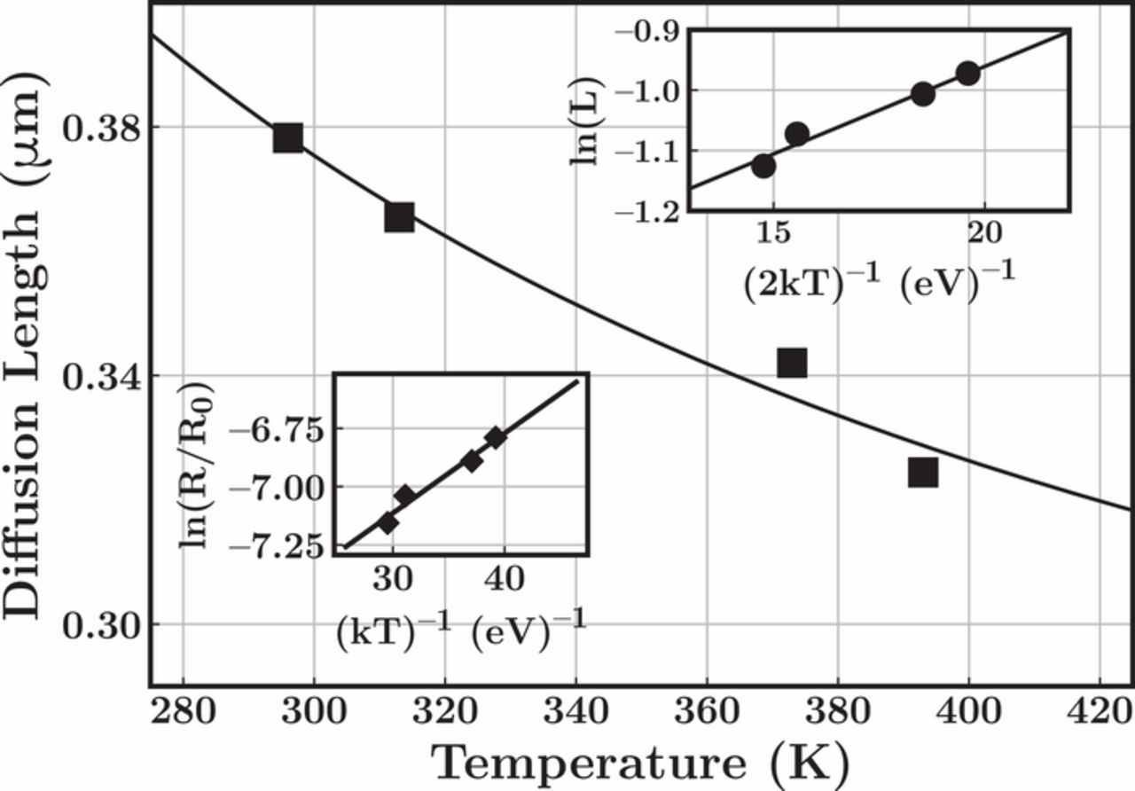
Figure 4. Temperature dependence of diffusion length for the alpha particle irradiated structure. Inset (top-right): Arrhenius plot for Equation 2, used in the calculation of activation energy for diffusion length change with temperature. Inset (bottom): Arrhenius plot for Equation 3, used in the calculation of activation energy for diffusion length change due to electron injection.
One can see from Figs. 3, 4, that for all temperatures, L for reference sample is greater than the same parameter for alpha-irradiated sample. This effect is attributed to generation of defects, providing more pathways for the carriers to recombine, and to creation of new scattering centers due to radiation damage.18 The activation energy for temperature dependent decrease of the diffusion length is calculated from the following equation,30,38
![Equation ([2])](https://content.cld.iop.org/journals/2162-8777/8/7/Q3050/revision1/d0002.gif)
where L is the diffusion length of minority carriers; L0 is the asymptotic diffusion length; T is the temperature in Kelvin; k is the Boltzmann constant; and ΔEA,T is the activation energy for temperature dependent L decrease. ΔEA,T, obtained as the slope of Arrhenius plot of Equation 2 (Figs. 3, 4 upper-right insets), for reference and alpha particle-irradiated structures are ∼53 meV30 and ∼29 meV, respectively. In previous studies,39,40 the activation energies of this magnitude have been associated with Si-donors (which form fairly shallow levels), and carrier thermalization being the likely cause of L reduction as a function of increasing temperature41 with carrier-phonon interaction being the dominant contributor.42,43
In this study, the impurity traps available for non-equilibrium carrier recombination are filled by electrons, thus stop participating in the recombination process.18 With increase in the duration of electron injection, more of these traps become unavailable for recombination. This, in turn, will lead to longer non-equilibrium carrier lifetime in the conduction and valence bands and, hence, elongated diffusion length. In the alpha-irradiated structure, in addition to the intrinsic defect states, more trap levels are introduced due to radiation damage. As compared to the reference structure, this results in slower saturation of these traps, due to electron injection by SEM beam, and lower rate of increase for diffusion length with electron injection duration (cf. Fig. 2, where the rate of diffusion length increase is a slope of L vs. injection duration dependence).
The activation energy associated with rate of increase of L due to electron injection is given by:30
![Equation ([3])](https://content.cld.iop.org/journals/2162-8777/8/7/Q3050/revision1/d0003.gif)
where R is the rate of L increase; R0 is a constant; ΔEA,T is thermal activation energy for diffusion length decrease (from Equation 2); k is the Boltzmann constant; T the is temperature in Kelvin; ΔEA,I is the activation energy due to electron injection effect. Similar to the Refs. 30,31 ΔEA,I obtained from the slope of the Arrhenius plot using Equation 3 (cf. lower-left inset in Fig. 3 for reference, and the same in Fig. 4 for alpha-irradiated structure) is respectively ∼74 meV31 and ∼49 meV for reference and alpha-irradiated structures. For the reference structure, similar results were obtained in an independent study and the origin of the traps, associated with this activation energy, is yet unknown.44 As a speculative suggestion, one could propose oxygen or oxygen-gallium vacancies or their higher order complexes due to oxygen displacement.45,46
Previous studies on the effect of proton radiation damage in a similar structure has attributed the decrease in thermal activation energy for the diffusion length, ΔEA,T, to generation of defect trap states between the shallow donor levels and the conduction band.18 Note that [ΔEA,T]Reference - [ΔEA,T]Irradiated ≈ 24 meV and [ΔEA,I]Reference - [ΔEA,I]Irradiated ≈ 25 meV are comparable. This indicates that the same radiation-induced traps are responsible for L decrease with increasing temperature and L increase with electron injection duration.
To summarize, the effect of electron injection on 18 MeV alpha particle irradiated Si-doped β-Ga2O3 is as follows:
- Electron injection with an electron beam causes generation of non-equilibrium electron-hole pairs in the material, but only minority carriers are collected and recorded.
- While the measured diffusion length of minority carriers (holes, in this case) decreases as temperature rises, L increases with the duration of electron injection.
- The activation energy for L increase due to electron injection is found to be ∼74 meV in the reference structure, which is associated with a trap level of yet unknown origin. For the irradiated structure, the activation energy is ∼49 meV.
- With the duration of electron injection, there is a rise in the number of trap levels occupied by non-equilibrium (generated by SEM beam) electrons. This results in unavailability of these levels for recombination, thus increasing the lifetime of carriers in conduction and valence bands.
- The phenomenon is valid for both reference and alpha-irradiated structures. In the latter case, radiation damage generates additional trap levels between the intrinsic trap states in the structure and the conduction band. These additional traps act as an efficient pathway for carrier recombination, triggering more recombination events and, hence, reducing the diffusion length of minority carriers, as compared to the reference structure.
- The difference between the activation energy for temperature dependence of L for the reference and irradiated structure is ∼24 meV. This value closely matches that for L change due to electron injection (∼25 meV). As a result, it can be concluded that same trap levels, generated due to radiation damage, play the role in both processes.
Conclusions
Radiation damage in Si-doped β-Ga2O3 shows low diffusion length compared to reference structure in the temperature range from 23°C to 120°C. The radiation damage is possibly associated with shallow oxygen vacancies, which serve as an energy efficient pathway for carrier recombination. The diffusion length can be significantly increased by electron injection for both reference and irradiated structures, though the rate of its increase is lower after irradiation. The effect of electron injection shows a great potential for mitigation of radiation induced defects.
Acknowledgments
Research at UCF and the Weizmann institute was supported in part by NATO (award # G5453) and NSF (UCF award # ECCS1802208). The work at UF was sponsored by the Department of Defense, Defense Threat Reduction Agency, HDTRA1-17-1-011, monitored by Jacob Calkins.
ORCID
Leonid Chernyak 0000-0001-7737-0251
Fan Ren 0000-0001-9234-019X
Stephen J. Pearton 0000-0001-6498-1256