
Abstract
A perfect crystalline phases of cuprous oxide were synthesized using electrochemical method at different duration ( 15, 30 and 60 min). The deposited samples were examined by XRD, SEM, UV–Vis absorption and Mott-Schottky measurements. The effect of the deposition time on the optical and dielectric properties of Cu2O was studied in detail. The x-ray diffraction indicated increasing of crystallinity and crystallite size with increasing of deposition time. SEM micrographs exhibited grains with three-faced pyramid shape and grains size increased with improvement of crystallinity. Optical study is performed to calculate optical band gap (Eg), absorption coefficient (α), extinction coefficient (k), refractive index (n), dielectric constants (ε), urbach energy (EU) and optical conductivity (σopt) using the transmittance and absorption spectra in the wavelength range of 400–1100 nm. Among all grown samples, the film deposited at 60 min shows interesting optical and dielectric properties. The Mott-Schottky analysis shows that the film deposited at 60 min has a low carrier density compared to samples deposited in other deposition times.
Export citation and abstract BibTeX RIS

Original content from this work may be used under the terms of the Creative Commons Attribution 4.0 licence. Any further distribution of this work must maintain attribution to the author(s) and the title of the work, journal citation and DOI.
1. Introduction
Cuprous oxide (Cu2O) is a p-type semiconductor and a promising candidate for solar energy conversion thanks to its good absorption coefficient in the visible range and its direct band gap of 2.1 eV [1, 2]. In addition, the Cu2O thin film has many advantages such as abundance and nontoxicity and low production cost [3]. Up to now, there have been several reports on various Cu2O-based solar cells [4, 5]. The theoretical energy conversion efficiency of Cu2O was found to be 20% [6]. Several methods are usually used to prepare Cu2O thin films, including pulsed laser deposition [7], sol gel [8], hydrothermal [9, 10], chemical bath deposition [11, 12], chemical vapor deposition [13], electrodeposition [14, 15] and spray pyrolysis [16]. Among these methods, electrodeposition is one of the most interesting methods for the synthesis of thin films of semiconductor oxides [14]. This technique allows to control the stoichiometry, thickness, and structure of Cu2O films by adjusting the deposition parameters such as temperature, pH, voltage and time deposition, thus the thin films could be highly ameliorated. According to the literature, Messaoudi et al [17] studied the effect of deposition time on Cu2O thin films in the range time of 5 min to 10 min, they observed a betterment in the crystallinity and grain size when the deposition time is increased, and they revealed that Cu2O films are suitable as photo-absorbers in the industrial applications. Hossain et al [18] have investigated the effect of deposition time on Cu2O thin films synthesized by electrodeposition method by using an aqueous precursor solution at room temperature. They found that the films are comprised of Cu2O nanoparticles with distinctive wavelike surface feature. Hanif [19] reported that deposition time affected the structural, morphological and topological properties of n-Cu2O thin films. From the above literature reviews, most of the works have reported on effect of deposition times on surface morphology, crystal quality properties of the Cu2O films. While in-depth studies of the effect of deposition time on optical and dielectric properties have rarely been reported. Therefore, the objective of this work is to study in detail the effect of the electrodeposition time on optical and dielectric properties of Cu2O thin films deposited at −0.5 V. Moreover, this work aims to optimize the properties of Cu2O thin films as absorber to make a Cu2O/ZnO NRs junctions.
2. Experimental
All experiments electrodeposition were conducted in a standard three electrode cell connected to potentiostat/galvanostat Autolab PGZ 301. In the electrochemical cell a working electrode consisting of FTO substrate with a surface area of 1 cm × 1.5 cm, the counter-electrode was platinum mesh and saturated calomel electrode (SCE) as a reference electrode. Before using, all FTO substrates were ultrasonically cleaned in acetone for 10 min, ethanol for 10 min and deionized water. The bath temperature was 60°C at a potential of −0.5 V versus SCE. The Cu2O thin films were deposited from an aqueous solution containing 0.2 M copper (II) sulfate (CuSO4.4H2O) and 3 M lactic acid (C3H6O3) as chelating agent, the pH of the bath was adjusted to 9 with sodium hydroxide (NaOH) in order to deposit p-type Cu2O [20]. The thin film deposition potential −0.5 V was determined from the results of the linear voltammetry measurement. The Cu2O thin films were analyzed through x-ray diffraction using a X'PERT-PRO diffractometer analysis with CuKα radiation (λ = 1.5406 Å). The surface morphology of Cu2O samples were investigated by using scanning electron microscope (FEIQuanta200). The transmittance and UV-Visible absorption spectra were recorded by a Jasco V-730 spectrophotometer. The spectra were recorded in the wavelength range from 400 to 1100 nm. The conductivity type of Cu2O films was characterized through Mott-Schottky measurements, the potential sweeps were carried out from −0.2 V to 0.6 V, the AC frequency used in the impedance measurements was 1000 Hz.
3. Results and discussion
3.1. Electrochemical characterization
Figure 1(a) shows the linear sweep voltammetry (LSV) curve of FTO substrate in a solution containing 0.2 M copper (II) sulfate and 3 M lactic acid with scan rate of 20 mV s−1, pH and temperature of the bath were maintained at values 9 and 60 °C respectively. The potential range is between −1.3 and 0 V versus SCE. It is clearly shown in the figure that there are two reduction regions. We were interested in the first region that was detected between −0.23 V and −0.6 V in which there is the deposition of cuprous oxide Cu2O according to the following mechanism [21]:


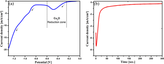
Figure 1. (a) Linear sweep voltammogram obtained from a bath (pH = 9) containing 0.2 M CuSO4 and 3 M lactic acid at 60 °C. (b) Current transients for Cu2O thin films deposited at different applied potentials.
Download figure:
Standard image High-resolution imageCu2O films were synthesized at the selected potential of −0.5 V. Figure 1(b) represents the shape of current transient of Cu2O thin films. The shape of the curve indicates clearly the nucleation-growth step [21], the curve exhibits three regions, the first region corresponding to the double-layer charging at the interface of FTO/electrolyte, in which the current density increases until the maximum current (Imax) is reached at a maximum time tmax. The second region corresponds to the nucleation and growth of Cu2O nuclei, in this step the cathodic current density decreases due to Cu2O film cover the surface. Finally, the cathodic current density value become steady with increase deposition time due to growth process of the Cu2O film on the FTO substrate.
3.2. Structural characterization
Figure 2 shows the XRD pattern of Cu2O thin films electrodeposited on the conductive substrate FTO at different time 15, 30 and 60 min, respectively. The several peaks shown by the XRD pattern confirm polycrystalline nature of Cu2O thin film which has cubic structure according the JCPDS N°: 05-0667 [22]. Moreover, the XRD patterns show obviously no secondary phases. The films deposited at 15, 30 and 60 min are oriented preferentially along [111] direction with lattice parameter a = 4.26 Å. When the deposition time is varied from 15 to 60 min, a clear increase of (111) peak intensity is observed indicating an improvement in the crystallinity of the films.
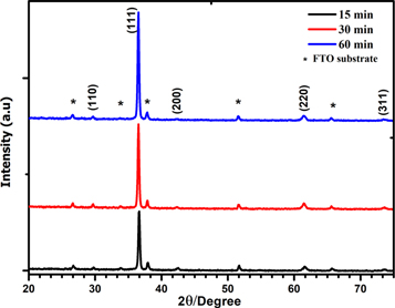
Figure 2. XRD patterns of the Cu2O films deposited at −0.5 V for 15, 30 and 60 min.
Download figure:
Standard image High-resolution imageThe crystallite size of the samples deposited was estimated by using Scherrer formula (equation (3)) [23].

Where D, k, λ, θ and β are the crystallite size, a constant equal to 0.9, the wavelength of the x-ray, the diffraction angle and the full width at half maximum (FWHM) of the diffraction peak, respectively.
The dislocation density (δ), defined as the length of dislocation lines per unit volume, was evaluated from the formula (equation (4)) [24]:

Strain (ε) of the films was calculated by the formula (equation (5)) [24]:

The calculated values of the lattice parameter, the crystallite size, the dislocation density and the microstrain are summarized in table 1. The calculated crystallite size is increased from 62.83 nm to 66.53 nm when the deposition time is varied from 15 to 60 min. While, the δ and ε decrease from 2.533 × 10⁻¹⁴ to 2.259 × 10⁻¹⁴ lines m−2 and 0.551 × 10⁻³ to 0.52 × 10⁻³, when increasing the deposition time from 15 to 60 min. This is due to a decrease in defect levels and grain boundaries as well as an increase in crystallite size [25].
Table 1. Microstructural parameters of the Cu2O thin films deposited at 15, 30 and 60 min.
| Deposition time | Lattice parameter a(Å) | FWHM (β) (×10−3 (rad)) | Grain size D (nm) | Dislocation density δ (×10−14) (lines m−2) | Strain ε (×10−3) (lines−2 m−4) |
|---|---|---|---|---|---|
| 15 min | 4.249 | 2.301 | 62.83 | 2.533 | 0.551 |
| 30 min | 4.259 | 2.213 | 65.29 | 2.345 | 0.530 |
| 60 min | 4.261 | 2.172 | 66.53 | 2.259 | 0.520 |
3.3. Morphological analysis
The SEM micrographs with two magnifications of each Cu2O thin films prepared at different deposition times of 15, 30 and 60 min are presented in the figures 3(a)–(c) respectively. The all micrographs clearly show that samples have a homogeneous distribution of high nanometric grains cover uniformly the surfaces, dense microstructures and void-free surface. In each sample, the grains are well defined, hierarchical shapes and inhomogeneously sized. It is worth noting that when deposition time increases, from 15 to 60 min, a noticeable increase in grain size is observed. In fact, the average grain size for the samples of 15, 30 and 60 min are 520, 670 and 850 nm respectively.
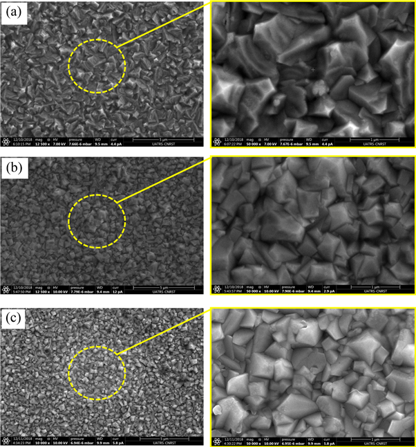
Figure 3. SEM images of the Cu2O films deposited at (a) 15 min, (b) 30 min and (c) 60 min.
Download figure:
Standard image High-resolution image3.4. Conductivity type of Cu2O films
The Mott-Schottky analysis was used to characterize the electrodeposited Cu2O films with different deposition time. The sign of Mott-Schottky plots identify the conductivity type of the deposited Cu2O films. A positive slope of the linear part of the curve presents n-type conductivity, while a negative slope indicates p-type conductivity [26]. The linear region of Mott-Schottky plots for the deposited Cu2O films at different time are shown in figure 4. All Cu2O films deposited at 15, 30 and 60 min exhibit negative slopes as shown in figure 4, indicating p-type conductivity. The origin of p-type conductivity of Cu2O films has basically been agreed on the formation of Cu vacancies [27, 28]. Mott-Schottky measurements used also to estimate the flat band potential (Vfb) and the carrier density, the equation is presented as [26]:

Where C, e, ε0, ε, NA, Vfb, V, T and k are the space-charge capacitance, the electron charge, the permittivity of free space, the relative permittivity, the carrier density, the flat band potential, the applied potential, the absolute temperature and the Boltzmann constant, respectively. The obtained carrier densities and the flat band potentials of the Cu2O films from the Mott-Schottky measurements are listed in table 2. The flat band potentials of the p-type Cu2O films increased from 0.438 V to 0.458 V with increasing of deposition time. The acceptor densities of the samples decrease with improvement of crystallinity. These results of carrier concentrations for Cu2O thin films are in good agreement with those reported in the literature [18, 29].

Figure 4. Mott-Schottky plots of the Cu2O films deposited at 15 min, 30 min and 60 min.
Download figure:
Standard image High-resolution imageTable 2. Carrier densities and flat band potentials of Cu2O films deposited at different deposition time.
| Deposition time | Conductivity type | Carrier density/cm−3 | Flat band potential/V |
|---|---|---|---|
| 15 min | p-type | 4.53 × 10¹⁸ | 0.438 |
| 30 min | p-type | 4.48 × 10¹⁸ | 0.443 |
| 60 min | p-type | 4.15 × 10¹⁸ | 0.458 |
3.5. Optical properties
Optical absorption studies are important to determine the optical band gap of semiconductor films, and for understanding the optoelectronic properties of our growing semiconductor. The absorbance spectra in the visible region of the deposited Cu2O thin films synthetized at different deposition times are displayed in figure 5(a). We observe from the showed spectra an absorption edge localized between 500 and 600 nm which corresponds to the excitonic band gap of Cu2O. Moreover, figure 5(b) illustrates that the sample electrochemically grown at 15 min exhibits a higher transmittance. We observe that the transmittance was significantly decreases with increasing of deposition time. The plots of (αhν)2 versus (hν) obtained from optical transmittance spectra for all samples is shown in figure 5(c). From the straight lines of plots of (αhν)2 versus (hν), we conclude that the deposited films have a direct forbidden band gaps. Using the linear extrapolation method, the values of band gap energy of Cu2O films deposited at 15, 30 and 60 min are estimated to be 2.32, 2.22 and 2.17 eV, respectively. Our finding results are in good agreement with literature data for Cu2O films prepared by both chemical and physical deposition approaches [22, 30, 31].

Figure 5. (a) Optical absorbance and (b) transmittance of Cu2O thin films for different deposition time. (c) Tauc's plot of electrodeposited Cu2O thin films. (d) Absorption coefficient (α) as a function of photon energy hν of Cu2O films.
Download figure:
Standard image High-resolution imageThe absorption coefficient α of Cu2O thin films was evaluated from the transmittance data using relation (equation (7)), where α, T and d are the absorption coefficient, the transmittance and the thickness of Cu2O films, respectively [32].

Figure 5(d) shows that the absorption coefficient increases with increasing growth time and showing a maximum value around 104 cm−1 in the visible range 2.4–3 eV. We conclude that when the deposition time increases, an enhancement in the absorption coefficient of Cu2O thin films is observed. The absorption coefficient is used to define the Urbach parameter (Eu) corresponding to the transitions between the extended states of the valence band and the localized states of the conduction band. The absorption coefficient is related to Urbach parameter by the following formula [33]:


The Urbach energy Eu is determined by plotting lnα versus photon energy (hυ) as shown in figure 6. The results are summarized in table 3, the Urbach energy decreases with increase of deposition time. Eg optical band gap values change inversely with Eu energy. The results of Urbach energy are comparable to those reported by authors interpreting it as the bandwidth of the states located within the band gap width.
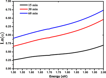
Figure 6. Urbach plots of Cu2O thin films deposited at different deposition time.
Download figure:
Standard image High-resolution imageTable 3. Urbach energy for Cu2O films.
| Deposition time | Urbach energy (eV) | Optical gap (eV) |
|---|---|---|
| 15 min | 0.749 | 2.32 |
| 30 min | 0.727 | 2.22 |
| 60 min | 0.709 | 2.17 |
The more critical optical constant of a semiconductor material is refractive index, its relationship with wavelength of incident light is known as dispersion name [34]. The refractive index is expressed as n = n* + ik, where n* is the complex refractive index, and k is imaginary refractive index also named as extinction coefficient as it indicates the total optical loss caused by transmittance and scattering. The n and k can be calculated from the following relations [34]:


where the parameters α, R and k are absorption coefficient, reflectance and extinction coefficient. Figures 7(a), (b) shows the refractive index (n) and the extinction coefficient (k) as a function of wavelength of the Cu2O films synthetized with different deposition times. We conclude that with increasing of wavelength, the refractive index and extinction coefficient values decrease, this is attributed to normal semiconducting dispersion behavior of the material. In other hand the extinction coefficients and refractive index values are influenced by the deposition time, and both increase with it. The slight increase can be attributed to an increase in density of the films with increasing deposition time. Table 4 shows the values of 'n' and 'k' on wavelength 1100 nm for all films. The found values are similar with the literature [35–37].

Figure 7. (a) Refractive index as a function of wavelength λ of Cu2O thin films. (b) Extinction coefficient as a function of wavelength λ of Cu2O thin films. (c) Real dielectric constant as a function of wavelength λ of Cu2O thin films. (d) Imaginary dielectric constant as a function of wavelength λ of Cu2O thin films.
Download figure:
Standard image High-resolution imageTable 4. The refractive index (n), extinction coefficient (k), real dielectric constant (εr), imaginary dielectric constant (εi) and optical conductivity (σopt) in the wavelength (λ = 1100 nm).
| Deposition time | n | k | εr | εi | σopt |
|---|---|---|---|---|---|
| 15 min | 2.13 | 0.0011 | 4.29 | 0.0095 | 1.03 × 10¹² |
| 30 min | 2.46 | 0.0018 | 5.86 | 0.0110 | 1.70 × 10¹² |
| 60 min | 2.89 | 0.0022 | 6.47 | 0.0145 | 2.32 × 10¹² |
In semiconductors the fundamental electronic transition is allied to the wavelength dependent complex dielectric constant, expressed as: εr + iεi. The real (εr) and imaginary parts (εi) of complex dielectric constant can be calculated from the extinction coefficient and refractive index using the following equations [38]:


The variation of real and imaginary dielectric constants as a function of the wavelength for thin films deposited at different time are presents in figures 7(c) and (d). It is observed that real and imaginary parts follow the same pattern, in the other hand the real values are higher than the imaginary values and both their values increases slightly with deposition time.
The optical conductivity allows to study conveniently the optical response. The optical conductivity (σopt) has been determined from the relation [38]:

where α, n and c are the absorption coefficient, the refractive index and the velocity of light, respectively. The plots of optical conductivity (σopt) as a function of photon energy for Cu2O films are shown in figure 8. We conclude that optical conductivity increases with increase of photon energy (hv) and deposition time. The increasing of σopt can be attributed to the increase of absorption coefficient (α) and refractive index (n). The increase in photon energy improves the movement of electrons, so the optical conductivity reaches the highest values. The values of 'εr', 'εi' and 'σopt' for different deposition time are calculated at the wavelength 1100 nm and listed in table 4.

Figure 8. Optical conductivity of Cu2O thin films as a function of photon energy (hν).
Download figure:
Standard image High-resolution image
4. Conclusion
In summary, Cu2O films were successfully elaborated on (FTO)-coated glass substrates at different deposition time using potentiostatic deposition. The electrodeposited films were analyzed for their structural, morphological, optical and dielectric properties. The XRD analysis revealed that Cu2O films crystalizes in a cubic structure with preferential orientation in the plane (111) and showed that the crystallinity and grain size were increased by increasing of deposition time. The SEM micrographs displayed three-sided pyramid-shaped grains, the uniformity and grains size increase with time deposition. The optical and dielectric properties of the films were calculated from the measurement optical of transmittance and absorbance. The optical energy band gap values were found to be 2.32, 2.22 and 2.17 eV at 15, 30 and 60 min respectively. Mott-Schottky measurements shows that all films are p-type semiconductors, the low carrier density attributed to the film deposited at 60 min. From this study, it is evident that the deposition time is an important key to obtain thin films suitable for solar cell applications