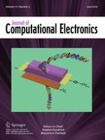
Top
Published in: Journal of Computational Electronics 2/2016

29-02-2016

Physics-based drain current modeling of gate-all-around junctionless nanowire twin-gate transistor (JN-TGT) for digital applications

Authors: Yogesh Pratap, Rajni Gautam, Subhasis Haldar, R. S. Gupta, Mridula Gupta

Published in: Journal of Computational Electronics | Issue 2/2016

Log in

Activate our intelligent search to find suitable subject content or patents.

search-config
loading …

Abstract

Vertically stacked dielectric separated independently controlled gates can be used to realize dual-threshold voltage on a single silicon channel MOS device. This approach significantly reduces the effective layout area and is similar to merging two transistors in series. This multiple independent gate device enables the design of new class of compact logic gates with low power and reduced area. In this paper, we present the junctionless concept based twin gate transistor for digital applications. To analyse the appropriate behaviour of device, this paper presents the modeling, simulation and digital overview of novel gate-all-around junctionless nanowire twin-gate transistor for advanced ultra large scale integration technology. This low power single MOS device gives the full functionality of “AND” gate and can be extended to full functionality of 2-input digital “NAND” gate. To predict accurate behaviour, a physics based analytical drain current model has been developed which also includes the impact of gate depleted source/drain regions. The developed model is verified using ATLAS 3D device simulator. This single channel device can function as “NAND” gate even at low operating voltage.

Dont have a licence yet? Then find out more about our products and how to get one now:

Springer Professional "Wirtschaft+Technik"

Online-Abonnement

Mit Springer Professional "Wirtschaft+Technik" erhalten Sie Zugriff auf:

  • über 102.000 Bücher
  • über 537 Zeitschriften

aus folgenden Fachgebieten:

  • Automobil + Motoren
  • Bauwesen + Immobilien
  • Business IT + Informatik
  • Elektrotechnik + Elektronik
  • Energie + Nachhaltigkeit
  • Finance + Banking
  • Management + Führung
  • Marketing + Vertrieb
  • Maschinenbau + Werkstoffe
  • Versicherung + Risiko

Jetzt Wissensvorsprung sichern!

Springer Professional "Technik"

Online-Abonnement

Mit Springer Professional "Technik" erhalten Sie Zugriff auf:

  • über 67.000 Bücher
  • über 390 Zeitschriften

aus folgenden Fachgebieten:

  • Automobil + Motoren
  • Bauwesen + Immobilien
  • Business IT + Informatik
  • Elektrotechnik + Elektronik
  • Energie + Nachhaltigkeit
  • Maschinenbau + Werkstoffe


Jetzt Wissensvorsprung sichern!

Springer Professional "Wirtschaft"

Online-Abonnement

Mit Springer Professional "Wirtschaft" erhalten Sie Zugriff auf:

  • über 67.000 Bücher
  • über 340 Zeitschriften

aus folgenden Fachgebieten:

  • Bauwesen + Immobilien
  • Business IT + Informatik
  • Finance + Banking
  • Management + Führung
  • Marketing + Vertrieb
  • Versicherung + Risiko


Jetzt Wissensvorsprung sichern!

Appendix
Available only for authorised users
Literature
1.
go back to reference Wong, H.S.P.: Beyond the conventional MOSFET. In: Proceeding of 31th European Solid State Device Research Conference, p. 69 (2011) Wong, H.S.P.: Beyond the conventional MOSFET. In: Proceeding of 31th European Solid State Device Research Conference, p. 69 (2011)
2.
go back to reference Lion, Y.B., Chaing, M.H., Damrongplasit, N., Hsu, W.C., Liu, T.J.K.: Design of gate-all-around silicon MOSFETs for 6-T SRAM area efficients and yield. IEEE Trans. Electron Dev. 61(7), 2371–2377 (2014)CrossRef Lion, Y.B., Chaing, M.H., Damrongplasit, N., Hsu, W.C., Liu, T.J.K.: Design of gate-all-around silicon MOSFETs for 6-T SRAM area efficients and yield. IEEE Trans. Electron Dev. 61(7), 2371–2377 (2014)CrossRef
3.
go back to reference Kaushal, G., Manhas, S.K., Maheshwaram, S., Anand, B., Dasgupta, S., Singh, N.: Novel design methodology using LEXT sizing in nanowire CMOS logic. IEEE Trans. Elect. Dev. 13(4), 650–658 (2014) Kaushal, G., Manhas, S.K., Maheshwaram, S., Anand, B., Dasgupta, S., Singh, N.: Novel design methodology using LEXT sizing in nanowire CMOS logic. IEEE Trans. Elect. Dev. 13(4), 650–658 (2014)
4.
go back to reference Lee, C., Zhuang, Y., Di, S., Han, R.: Subthreshold behavior models for nanoscale short-channel junctionless cylindrical surrounding-gate MOSFETs. IEEE Electron Dev. Lett. 60(11), 3655–3662 (2013)CrossRef Lee, C., Zhuang, Y., Di, S., Han, R.: Subthreshold behavior models for nanoscale short-channel junctionless cylindrical surrounding-gate MOSFETs. IEEE Electron Dev. Lett. 60(11), 3655–3662 (2013)CrossRef
5.
go back to reference Nayak, K., Bajaj, M., Konar, A., Oldiges, P.J., Natori, K., Iwani, H., Murli, K.V.R.M., Rao, V.R.: CMOS logic device and circuit performance of Si gate all around nanowire MOSFET. IEEE Trans. Electron Dev. 61(9), 3066–3074 (2014)CrossRef Nayak, K., Bajaj, M., Konar, A., Oldiges, P.J., Natori, K., Iwani, H., Murli, K.V.R.M., Rao, V.R.: CMOS logic device and circuit performance of Si gate all around nanowire MOSFET. IEEE Trans. Electron Dev. 61(9), 3066–3074 (2014)CrossRef
6.
go back to reference Wang, T., Lou, L., Lee, C.: A junctionless gate-all-around silicon nanowire FET of high linearity and its potential applications. IEEE Electron Dev. Lett. 34(4), 478–480 (2013)CrossRef Wang, T., Lou, L., Lee, C.: A junctionless gate-all-around silicon nanowire FET of high linearity and its potential applications. IEEE Electron Dev. Lett. 34(4), 478–480 (2013)CrossRef
7.
go back to reference Lee, C.W., Borne, A., Ferain, I., Afzalian, A., Yan, R., Akhavan, N.D., Razavi, P., Colinge, J.P.: High-temperature performance of silicon junctionless MOSFETs. IEEE Trans. Electron Dev. 57(3), 620–625 (2010)CrossRef Lee, C.W., Borne, A., Ferain, I., Afzalian, A., Yan, R., Akhavan, N.D., Razavi, P., Colinge, J.P.: High-temperature performance of silicon junctionless MOSFETs. IEEE Trans. Electron Dev. 57(3), 620–625 (2010)CrossRef
8.
go back to reference Doria, R.T., Pavanello, M.A., Trevisoli, R.D., Souza, M., Lee, C.W., Ferain, I., Akhavan, N., Yan, R., Razavi, P., Yu, R., Kranti, A., Colinge, J.P.: Analog operation temperature dependence of nMOS junctionless transistors focusing on harmonic distortion. J. Int. Circuit Syst. 6(5), 114–120 (2011) Doria, R.T., Pavanello, M.A., Trevisoli, R.D., Souza, M., Lee, C.W., Ferain, I., Akhavan, N., Yan, R., Razavi, P., Yu, R., Kranti, A., Colinge, J.P.: Analog operation temperature dependence of nMOS junctionless transistors focusing on harmonic distortion. J. Int. Circuit Syst. 6(5), 114–120 (2011)
9.
go back to reference Mathew, L., Du, Y., Thean, A.V.Y., Sadd, M., Vandooren, A., Prher, C., Steehehens, T., et al.: CMOS vertical multiple independent gate field effect transistor (MIGFET). In: Proceeding of IEEE International SOI Conference, pp. 187–189 (2004) Mathew, L., Du, Y., Thean, A.V.Y., Sadd, M., Vandooren, A., Prher, C., Steehehens, T., et al.: CMOS vertical multiple independent gate field effect transistor (MIGFET). In: Proceeding of IEEE International SOI Conference, pp. 187–189 (2004)
10.
go back to reference Mathew, L., Du, Y., Kalpat, S., Sadd, M., Zavala, M., et al.: Multiple independent gate field effect transistor (MIGFET)-Multi-Fin RF mixer architecture, three independent gates (MIGFET-T) operation and temperature characteristics beyond the conventional MOSFET. In: Proceeding of 31th Symposium on VLSI Technology Digest of Technical Papers Conference, pp. 200–201, (2005) Mathew, L., Du, Y., Kalpat, S., Sadd, M., Zavala, M., et al.: Multiple independent gate field effect transistor (MIGFET)-Multi-Fin RF mixer architecture, three independent gates (MIGFET-T) operation and temperature characteristics beyond the conventional MOSFET. In: Proceeding of 31th Symposium on VLSI Technology Digest of Technical Papers Conference, pp. 200–201, (2005)
11.
go back to reference Rostami, M., Mohanram, K.: Dual-Vth independent gate FinFets for low power logic circuits. IEEE Trans. Electron Dev. 58, 567–571 (2011)CrossRef Rostami, M., Mohanram, K.: Dual-Vth independent gate FinFets for low power logic circuits. IEEE Trans. Electron Dev. 58, 567–571 (2011)CrossRef
12.
go back to reference Xiang, L., Chen, Z., Shen, N., Singh, N., Banerjee, K., Lo, G.Q., Knong, D.L.: Vertically stacked and independently controlled twin-gate MOSFETs on a single silicon nanowire. IEEE Electron Dev. Lett. 32(11), 1492–1494 (2011)CrossRef Xiang, L., Chen, Z., Shen, N., Singh, N., Banerjee, K., Lo, G.Q., Knong, D.L.: Vertically stacked and independently controlled twin-gate MOSFETs on a single silicon nanowire. IEEE Electron Dev. Lett. 32(11), 1492–1494 (2011)CrossRef
13.
go back to reference Zhang, J., Gaillardon, P.E., Micheli, G.: Dual-threshold voltage configurable circuits with three independent gate silicon nanowire FETs. IEEE Trans. Electron Dev. 58, 567–571 (2013) Zhang, J., Gaillardon, P.E., Micheli, G.: Dual-threshold voltage configurable circuits with three independent gate silicon nanowire FETs. IEEE Trans. Electron Dev. 58, 567–571 (2013)
14.
go back to reference Jeon, D.Y., Park, S.J., Mouis, M., Barraud, S., Kim, G.T., Ghibaudo, G.: Low-temperature electrical characterization of junctionless transistors. Solid State Electron. 80, 135–141 (2013)CrossRef Jeon, D.Y., Park, S.J., Mouis, M., Barraud, S., Kim, G.T., Ghibaudo, G.: Low-temperature electrical characterization of junctionless transistors. Solid State Electron. 80, 135–141 (2013)CrossRef
15.
go back to reference Colinge, J.P., Lee, C.W., Afzalian, A., Akhavan, N.D., Yan, R., Ferain, I., Razavi, P., Neill, B.O., Blake, A., White, M., Kelleher, A.M., McCarthy, B., Murphy, R.: Nanowire transistors without junctions. Nat. Nanotechnol. 5(3), 225–229 (2010)CrossRef Colinge, J.P., Lee, C.W., Afzalian, A., Akhavan, N.D., Yan, R., Ferain, I., Razavi, P., Neill, B.O., Blake, A., White, M., Kelleher, A.M., McCarthy, B., Murphy, R.: Nanowire transistors without junctions. Nat. Nanotechnol. 5(3), 225–229 (2010)CrossRef
16.
go back to reference Ghosh, D., Parihar, M., Armstrong, G., Kranti, A.: High-performance junctionless MOSFETs for ultralow-power analog/RF applications. IEEE Electron Dev. Lett. 33(10), 1477–1479 (2012)CrossRef Ghosh, D., Parihar, M., Armstrong, G., Kranti, A.: High-performance junctionless MOSFETs for ultralow-power analog/RF applications. IEEE Electron Dev. Lett. 33(10), 1477–1479 (2012)CrossRef
17.
go back to reference Doria, R.T., Pavanello, M., Trevisoli, R.D., Souza, M., et al.: Junctionless multiple-gate transistors for analog applications. IEEE Trans. Electron Dev. 58(8), 2511–2519 (2011)CrossRef Doria, R.T., Pavanello, M., Trevisoli, R.D., Souza, M., et al.: Junctionless multiple-gate transistors for analog applications. IEEE Trans. Electron Dev. 58(8), 2511–2519 (2011)CrossRef
18.
go back to reference Pratap, Y., Haldar, S., Gupta, R.S., Gupta, M.: Localised charge dependent threshold voltage analysis of gate-material-engineered junctionless nanowire transistor. IEEE Trans. Electron Dev. 62(8), 2598–2605 (2015)CrossRef Pratap, Y., Haldar, S., Gupta, R.S., Gupta, M.: Localised charge dependent threshold voltage analysis of gate-material-engineered junctionless nanowire transistor. IEEE Trans. Electron Dev. 62(8), 2598–2605 (2015)CrossRef
19.
go back to reference Moon, D.I., Choi, S.J., Duarte, J.P., Choi, Y.K.: Investigation of silicon nanowire gate all around junctionless transistors built in bulk substrate. IEEE Trans. Electron Dev. 60(4), 1355–1359 (2013)CrossRef Moon, D.I., Choi, S.J., Duarte, J.P., Choi, Y.K.: Investigation of silicon nanowire gate all around junctionless transistors built in bulk substrate. IEEE Trans. Electron Dev. 60(4), 1355–1359 (2013)CrossRef
20.
go back to reference Pratap, Y., Haldar, S., Gupta, R.S., Gupta, M.: Performance evaluation and reliability issues of junctionless CSG MOSFET for RFIC design. IEEE Trans. Dev. Mater. Reliab. 14(1), 418–425 (2014)CrossRef Pratap, Y., Haldar, S., Gupta, R.S., Gupta, M.: Performance evaluation and reliability issues of junctionless CSG MOSFET for RFIC design. IEEE Trans. Dev. Mater. Reliab. 14(1), 418–425 (2014)CrossRef
21.
go back to reference SILVACO Int. Santa Clara, CA.: ATLAS 3D device simulator (2014) SILVACO Int. Santa Clara, CA.: ATLAS 3D device simulator (2014)
22.
go back to reference Cong, L., Yiqi, Z., Ru, H.: New analytical threshold voltage model for halo-doped cylindrical surrounding-gate MOSFETs. J. Semicond. 32(7), 1–8 (2011) Cong, L., Yiqi, Z., Ru, H.: New analytical threshold voltage model for halo-doped cylindrical surrounding-gate MOSFETs. J. Semicond. 32(7), 1–8 (2011)
23.
go back to reference Chiang, T.K.: A compact model for threshold voltage of surrounding-gate MOSFETs with localised interface trapped charges. IEEE Trans. Electron Dev. 58, 567–571 (2011)CrossRef Chiang, T.K.: A compact model for threshold voltage of surrounding-gate MOSFETs with localised interface trapped charges. IEEE Trans. Electron Dev. 58, 567–571 (2011)CrossRef
24.
go back to reference Pratap, Y., Ghosh, P., Haldar, S., Gupta, R.S., Gupta, M.: An analytical subthreshold current modeling of cylindrical gate all around (CGAA) MOSFET incorporating the influence of device design engineering. Microelectron. J. 45(4), 408–415 (2014)CrossRef Pratap, Y., Ghosh, P., Haldar, S., Gupta, R.S., Gupta, M.: An analytical subthreshold current modeling of cylindrical gate all around (CGAA) MOSFET incorporating the influence of device design engineering. Microelectron. J. 45(4), 408–415 (2014)CrossRef
25.
go back to reference Choi, S.J., Moon, D.I., Kim, S., Duarte, J.P., Choi, Y.K.: Sensitivity of threshold voltage to nanowire width variation in junctionless transistors. IEEE Electron Dev. Lett. 32, 125–132 (2011)CrossRef Choi, S.J., Moon, D.I., Kim, S., Duarte, J.P., Choi, Y.K.: Sensitivity of threshold voltage to nanowire width variation in junctionless transistors. IEEE Electron Dev. Lett. 32, 125–132 (2011)CrossRef
26.
go back to reference Kumari, V., Saxena, M., Gupta, R.S., Gupta, M.: Two-dimensional analytical drain current model for double-gate MOSFET incorporating dielectric pocket. IEEE Trans. Electron Dev. 59(10), 2567–2574 (2012)CrossRef Kumari, V., Saxena, M., Gupta, R.S., Gupta, M.: Two-dimensional analytical drain current model for double-gate MOSFET incorporating dielectric pocket. IEEE Trans. Electron Dev. 59(10), 2567–2574 (2012)CrossRef
Metadata
Title
Physics-based drain current modeling of gate-all-around junctionless nanowire twin-gate transistor (JN-TGT) for digital applications
Authors
Yogesh Pratap
Rajni Gautam
Subhasis Haldar
R. S. Gupta
Mridula Gupta
Publication date
29-02-2016
Publisher
Springer US
Published in
Journal of Computational Electronics / Issue 2/2016
Print ISSN: 1569-8025
Electronic ISSN: 1572-8137
DOI
https://doi.org/10.1007/s10825-016-0798-1

Other articles of this Issue 2/2016

Journal of Computational Electronics 2/2016 Go to the issue